Signal integrity analysis model
In order to perform circuit simulation, it is necessary to first build a model of the component, that is, for the various components supported by the circuit simulation program, there must be a corresponding mathematical model to describe them in the simulation program, that is, a calculation formula that can be calculated by a computer. To express them. An ideal component model should reflect both the electrical characteristics of the component and the numerical solution on the computer. In general, the higher the accuracy of the device model, the more complex the model itself, and the more the number of model parameters required. In this way, the amount of memory occupied increases and the calculation time increases. While integrated circuits often contain a large number of components, a slight increase in the complexity of the device model can double the computation time. Conversely, if the model is too rough, the analysis results will be unreliable. Therefore, the complexity of the component model used depends on actual needs.


 NextPCB Capabilities
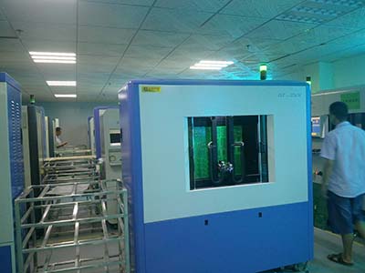
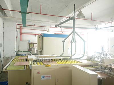
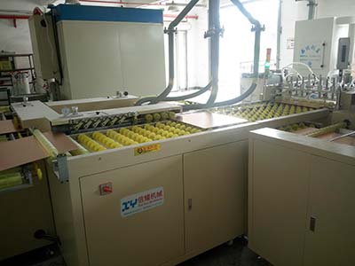
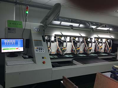
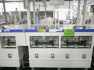
 PCB Assembly
 Layer Buildup
 SMD-Stencils
 PCB Design-Aid & Layout
 Mechanics
 Surface
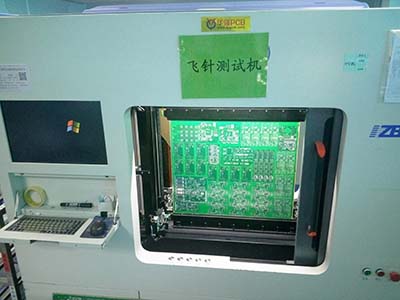
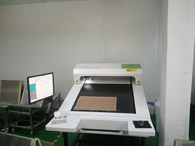
 Quality
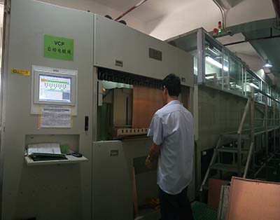
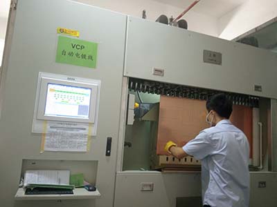
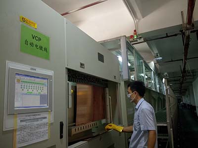
 Drills & Throughplating
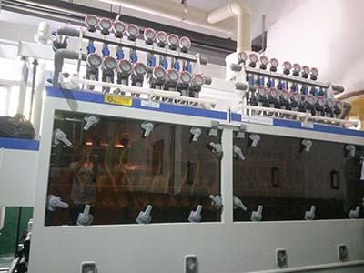
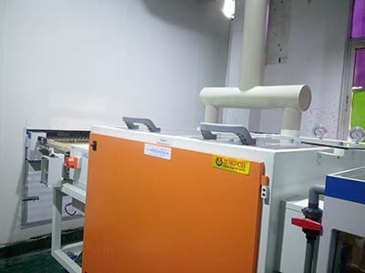
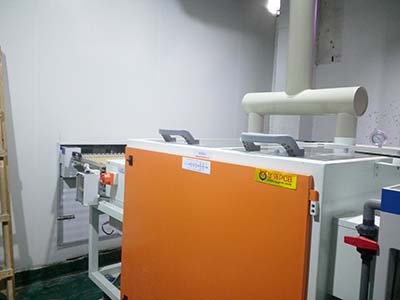
 Factory & Certificate