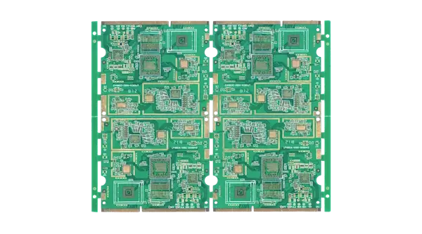
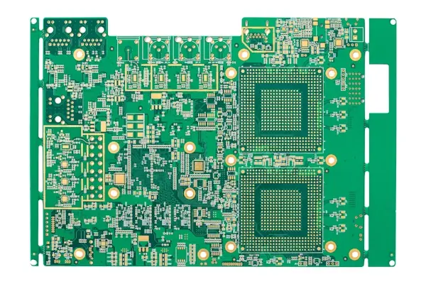
NextPCB Capabilities
Printed Circuit Boards
NextPCB Capabilities
Printed Circuit Boards
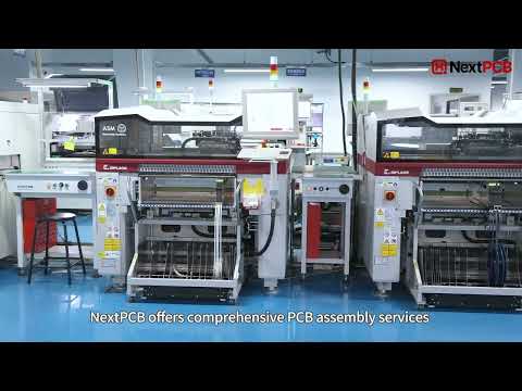
 PCB Assembly
 Layer Buildup
 SMD-Stencils
 PCB Design-Aid & Layout
 Mechanics
 Quality
 Drills & Throughplating
 Factory & Certificate
 PCB Assembly Factory Show
Certificate
PCB Assembly Factory Show
Certificate
Support Team
Feedback:
support@nextpcb.com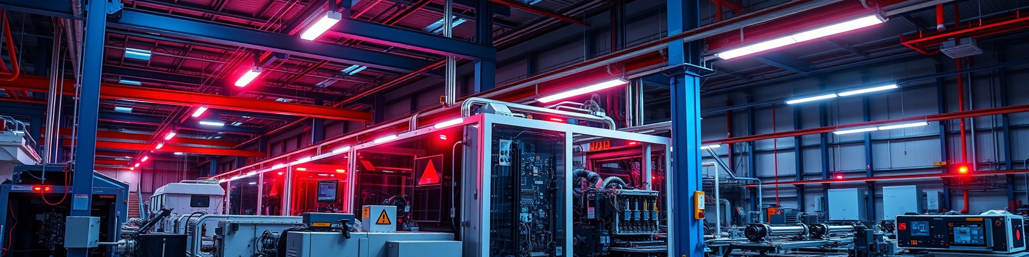
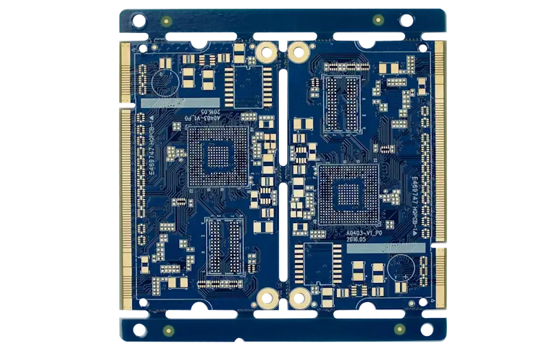
From 3/3 mil HDI to Complex Rigid-Flex. IPC Class 3 & IATF16949 certified manufacturing engineered for absolute reliability.
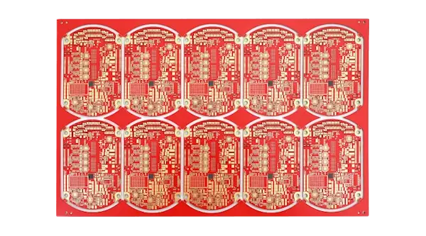
Cutting-edge PCB solutions for prototyping and mass production, from simple single-layer boards to complex HDI and specialized substrate PCBs.
| FR4 PCB Specifications: Detailed technical specifications for complex designs. | |
|---|---|
| Circuit Layers | Up to 32 layers |
| HDI Blind/Buried Vias | Up to HDI III designs |
| Base Material | Rogers, Isola, TUC, EMC and ITEQ laminates |
| Surface Finishes | HASL, Lead Free HASL, ENIG, OSP, Hard Gold, Electrolytic Gold, Gold Fingers, Immersion Tin, Immersion Silver and ENEPIG. |
| Copper Thickness | Up to 10 oz |
| Min. Trace Width/Spacing | 2.5/2.5 mil |
| Drill and Via Capabilities | Blind/buried vias, microvias, Via-in-pad fill and cap (POFV), castellated holes, counterbore/countersunk holes, z-axis milling, 20:1 aspect ratio and more. |
| PCB Solder Mask Color | Matte green, purple, orange, clear, custom solder mask colors. |
| Extras | Custom stack-up, impedance control, microsection report, IPC Class 3, UL Marking, beveled/chamferred edges, edge-plating and more. |
>> If your requirement isn't listed, our engineering team provides custom stack-up solutions.
Select a board technology to explore our detailed manufacturing parameters and engineering limits.
Strict dielectric control (Dk/Df) and specialized plating designed for 5G telecommunications, millimeter-wave radars, and advanced RF modules.
| Preferred Materials | Rogers 4000/3000 Series, Taconic, PTFE |
| Impedance Control Tol. | ±5% (Custom Process available) |
| Hybrid Stack-ups | Fully Supported (e.g., Rogers + High-Tg FR4) |
| Edge Plating / Castellated Holes | Supported (For EMI shielding integration) |
| Surface Finish Recommendation | Immersion Silver / Hard Gold (Low insertion loss) |
Industry-leading high-frequency laminates for aerospace, defense, and carrier-grade infrastructure. NextPCB offers expert handling of Rogers 4350B, 4003C, and 3000 series with optimized bonding processes.
| Common Stock | RO4350B, RO4003C, RO4835, RO3003, RO3006 |
| Dielectric Constant (Dk) | 2.55 - 10.2 (±0.05 stability) |
| Dissipation Factor (Df) | 0.0013 - 0.0037 @ 10GHz |
| Layer Bonding | FR4 Hybrid (Cost-effective) or Pure Rogers Multi-layer |
| Drilling Process | Plasma Desmear required for PTFE-based (3000 series) |
Optimized for Signal Integrity (SI) in high-bandwidth applications like data centers and servers. Featuring controlled backdrilling to minimize stub capacitance.
| Advanced Materials | Panasonic Megtron 4/6/7, Isola, TU-872 |
| Backdrilling Stub Remaining | Max 8-10 mil (0.2 - 0.25 mm) |
| Differential Impedance Tol. | ±8% to ±10% |
| Max Layer Count | Up to 40 Layers |
| Via-in-Pad (VIPPO) | Supported for fine-pitch BGA breakouts |
For Advanced Custom Fabrication tier: We recommend a DFM review with our senior engineers to guarantee Signal Integrity (SI) and manufacturing feasibility.
Exceptional dimensional stability and thermal reliability for severe environments. IPC-4101E compliant, perfect for automotive and industrial controls under lead-free reflow.
| Tg Value Options | Tg 170°C, Tg 180°C, up to Tg 210°C |
| Decomposition Temp (Td) | ≥ 340°C |
| Z-axis CTE | ≤ 3.0% (Excellent through-hole reliability) |
| Max Board Size | 20" x 24" (500x600mm) |
| Water Absorption Rate | ≤ 0.15% |
Enabling ultra-miniaturization with laser-drilled microvias. Supporting ELIC (Every Layer Interconnect) for smartphones, IoT, and tight-pitch BGA packaging.
| HDI Structures Supported | Up to HDI III designs, Any-Layer HDI (ELIC) |
| Min Trace Width / Space | 2.0 mil / 2.0 mil (0.05mm) |
| Min Laser Drill (Microvia) | 0.075 mm (3 mil) |
| Via Fill Technology | Conductive / Non-Conductive Resin + Plated Over |
| Microvia Aspect Ratio | Max 0.8:1 to 1:1 |
| Registration Tolerance | ±2 mil |
Superior current carrying capacity and excellent thermal dissipation, engineered specifically for EV charging systems, solar inverters, and power electronics.
| Max Outer Copper Thickness | Up to 10 oz+ |
| Max Inner Copper Thickness | Up to 4 oz - 6 oz |
| Min Trace/Space (for 3oz Cu) | 8 mil / 8 mil |
| Thermal Management | Thermal Coins, Copper Inlays, Thick Thermal Vias |
| Solder Mask Application | Double/Triple coatings for optimal edge coverage |
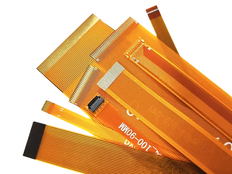
High-flexibility Polyimide circuits designed for dynamic bending environments and space-constrained enclosures like medical wearables and compact optics.
| Base Material Options | Adhesiveless PI, Adhesive PI |
| Min Trace Width / Space | 1.5 mil / 1.5 mil (Advanced) |
| Dynamic Bending Cycles | > 100,000 Cycles (Adhesiveless) |
| Stiffener Materials | FR4, Polyimide (PI), Stainless Steel (SUS) |
| EMI Shielding | Silver Ink, Conductive Film, Copper Foil |
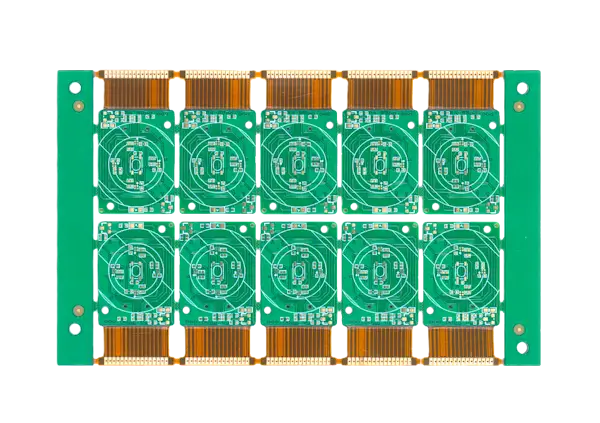
Combining the rigidity of FR4 with the 3D versatility of Polyimide. Eliminates external connectors for maximum reliability in aerospace and military hardware.
| Max Layer Count (Rigid) | Up to 20 Layers |
| Max Layer Count (Flex) | Up to 8 Layers |
| Flex Material Transition | Precise Tear-stop design & Acrylic/Epoxy adhesive |
| Min Mechanical Drill | 0.15 mm (6 mil) |
| Surface Finish Recommendation | ENIG (Ideal for bending stress & wire bonding) |
| Compliance standard | IPC-6013 Class 3 Capable |
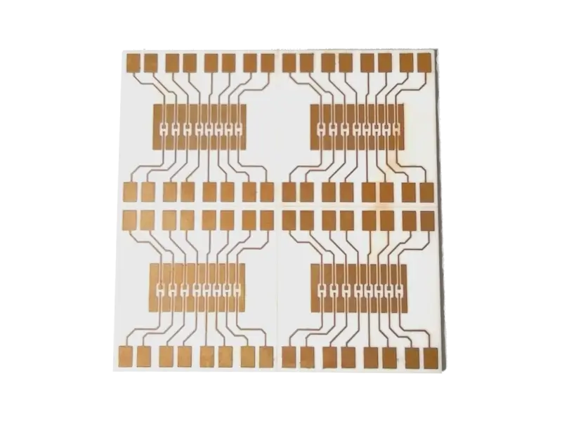
Delivering unparalleled thermal conductivity and zero moisture absorption. The ultimate solution for high-power LEDs, laser modules, and automotive sensors.
| Base Material Options | Alumina (Al2O3), Aluminum Nitride (AlN) |
| Thermal Conductivity | 24 W/m·K (Al2O3) to 170 W/m·K (AlN) |
| Conductor Thickness | 10μm to 300μm (DPC/DBC processes) |
| Max Board Size | Typically 115x115mm (4.5"x4.5") |
| Coefficient of Thermal Exp. (CTE) | Matches closely with bare die/semiconductors |
Custom PCB fabrication from high-thermal ceramic substrates to ultra-dense HDI interconnects, discover how our specialized board technologies solve your toughest engineering challenges.
Printed circuit boards made with high glass transition temperature (Tg) materials, typically 170°C and above.
PCBs designed to handle signals in the GHz range with minimal signal loss and distortion.
Circuit boards optimized for high-speed digital signals with careful attention to signal integrity.
High Density Interconnect PCBs with finer lines, smaller vias, and higher connection density.
PCBs manufactured using Rogers Corporation's high-performance laminate materials.
PCBs with exceptionally thick copper layers, typically 3 oz or more, for high-current applications.
Bendable PCBs made using polyimide or polyester substrates that can conform to dynamic or space-constrained designs.
Hybrid circuit boards that combine rigid and flexible substrates into a single integrated assembly.
Circuit boards manufactured using ceramic substrates like Al₂O₃ and AlN for extreme thermal and electrical performance.
From cutting-edge technology to medical-grade quality, we eliminate mass production risks.
Industry-leading specs for complex designs
Meeting strict AVL and audit requirements
Original CoC & full batch traceability
No request is too extravagant. Backdrilling? Embedded coins? Hybrid PCBs? Try us and see if we support your special processing needs.
| Feature | Standard PCBs | Advanced PCBs |
|---|---|---|
| Material Selection | Standard Kingboard or Shengyi FR-4 laminates | Rogers, Megatron, ITEQ, Isola and more |
| Layer Count | 1-20 layers | Up to 32+ layers |
| Special Processes | Basic - special processes may cause delays | Advanced tailored options |
| Applications | Consumer electronics, DIY projects, automotive | Medical, automotive, aerospace, high-frequency systems |
| Costs | Low - $5 USD for 5 pieces or even less | High - From less than one hundred to thousands |
| Production Time | Short - from 24 hours | Long - few days to weeks depending on complexity |
Professional engineers available
+86 755 8364 3663
WeChat & Online Chat
+86 13622941920
Expert answers to common engineering and manufacturing queries regarding our advanced PCB fabrication and EMS solutions.
We manufacture HDI PCBs up to 32 layers utilizing Any-Layer via technology. Our advanced laser drilling supports microvias down to 0.1mm (4mil). We offer blind, buried, and stacked vias compliant with IPC-6012 Class 3 standards, ensuring superior signal integrity and reliability for complex, high-speed designs.
We provide strict impedance control with a standard tolerance of ±10%, and can achieve ±5% tolerance for advanced high-speed and RF/Microwave applications upon request. We utilize TDR (Time Domain Reflectometry) testing on all impedance-controlled batches and provide detailed test reports to guarantee signal performance.
Absolutely. As an IATF 16949 and ISO 9001 certified manufacturer, we meet stringent automotive and industrial traceability requirements. We stock a comprehensive range of advanced substrates including Rogers (e.g., RO4350B), Teflon (PTFE), Polyimide (for Flex/Rigid-Flex), and high-Tg FR4 to support high-frequency and high-thermal applications.
Yes, our Turnkey PCBA service covers everything from fabrication to global component sourcing via authorized distributors. Our automated SMT lines support passive components down to 01005 imperial (0402 metric) and ultra-fine pitch BGAs (0.25mm pitch). Every board undergoes rigorous 3D SPI, 3D AOI, and optional X-ray inspection to ensure zero-defect assembly.
We offer seamless scalability. Rapid prototypes can be turned around in as fast as 24 hours. For mass production, our expert DFM (Design for Manufacturing) engineering team proactively reviews your Gerbers/ODB++ to optimize yield and reduce costs. Supported by our robust ERP tracking, standard volume production lead times are highly competitive and reliable.

 Surface