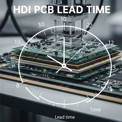
How HDI Impacts PCB Lead Time?
Concerned about the lead time for your High-Density Interconnect (HDI) PCBs? Ever wondered why your 14-layer, 3-stack HDI board might take 30 working days to deliver?While factors like layer count, impedance, and stack-up generally impact PCB lead times, HDI's unique complexity plays a crucial role. This article dives deep into how HDI processes affect PCB lead time, exploring specific production steps that extend schedules and how different HDI structures (e.g., 1-stack, 2-stack, 3-stack) directly influence delivery. We'll also provide practical tips on optimizing HDI structures to effectively shorten your lead time, helping you better estimate and manage project timelines in PCB design and procurement.


