Introduction
Modern electronics live or die by the quality of their assembly data. A PCB Assembly Drawing (AD) is more than a picture of parts—it's the single source of truth that links design intent to real-world manufacturing. In this guide, we unpack what a "good" AD looks like and why it directly drives first-pass yield, cost, and reliability. You'll learn how to specify coordinates (X/Y/θ), fiducials, polarity and RefDes conventions; how to separate Assembly vs. Silkscreen layers for readability and DFM; and how unified datasets like ODB++/IPC-2581 reduce errors across SMT placement, AOI/SPI/AXI, and test. We also cover advanced cases—HDI, rigid-flex, and 3D/STEP visualization—plus a printable submission checklist. Whether you're taping out your first board or optimizing a mature product line, this article gives you practical patterns to de-risk builds and accelerate time-to-market with NextPCB's expert DFM/DFA support.

NextPCB DFM Tool Exclusive Offer: Get a $10 Coupon Every Month!
Table of Contents
- I. The Strategic Role of Assembly Drawings
- II. Fundamental Elements: Core Information in the Assembly Drawing
- III. Standardization and DFM Practices
- IV. Error Types and Prevention
- V. Advanced Design: HDI, Rigid-Flex, and 3D Views
- VI. Digital Transformation: Tools and Data Formats
- VII. Process Synergy: Assembly Drawings and Production Lines
- VIII. Case Study: Optimization in Complex Projects
- IX. Future Outlook: Intelligent and Automated Drawings
- X. Conclusion and Recommendations
I. The Strategic Role of Assembly Drawings in the PCBA Ecosystem
What is Printed Circuit Board Assembly Drawing and Why PCB Assembly Drawings are Critical?
A Printed Circuit Board Assembly Drawing (PCB AD) serves as the "engineering language" that translates electronic design intent into an actual manufacturing process. It goes beyond defining the bare board's geometry (Fabrication Data) and focuses specifically on guiding the correct assembly of components. The core value of an Assembly Drawing lies in ensuring the precise orientation, accurate placement, and overall Design for Assembly (DFA) of the components. In modern, complex PCBA manufacturing processes, the Assembly Drawing is a crucial tool for guiding component placement, soldering, testing, and Quality Control (QC). A high-quality Assembly Drawing provides clear visual references for the manufacturing process, significantly improving accuracy and reducing production costs.
Defining Boundaries: Assembly Drawings vs. Gerber/Fabrication Data
Within the PCBA manufacturing data package, two main types of data exist, which are distinct yet complementary. Fabrication Data, such as Gerber RS-274X files, drill files, and stack-up documents, is primarily intended for the bare PCB manufacturer, focusing on defining the physical geometry, copper layer patterns, solder mask, and tolerances of the board.
In contrast, Assembly Data focuses on component assembly information, centrally including precise component locations (X/Y/θ coordinates), polarity identifiers, and the relationship to the Bill of Materials (BOM).
> Recommend reading: HQ Online Free Bill of Materials (BOM) Parts Matching and BOM Checker Tool
The industry is undergoing a major shift in data models. Traditional manufacturing relies on a multi-file delivery model: Assembly Drawing (PDF/DWG), Gerber files, the BOM, and Pick & Place (PnP) files. This file-group approach often leads to data fragmentation and human correlation errors. Gerber (including X2) remains primarily an image layer file and does not natively contain assembly data like BOM or coordinates; drill data must be provided separately via Excellon. While Gerber X2 adds attributes to carry some component/netlist metadata (like RefDes/Pin/Net), it is not a unified container, and assembly still relies on separate PnP/BOM files.
Conversely, modern data formats like ODB++ and IPC-2581 have evolved into unified data packages. These advanced formats integrate bare board fabrication, layer stack-up, drill information, BOM, component coordinates, and test information into a single structured file, thereby minimizing errors arising from data inconsistency and establishing the foundation for automated manufacturing.
|
Data Type
|
Target User
|
Core Information
|
Common Format
|
|
Fabrication Data
|
Bare PCB Manufacturer
|
Copper patterns, Solder mask, Drilling, Stack-up, Tolerances
|
Gerber RS-274X, Drill Files, Stackup PDF
|
|
Assembly Data
|
PCBA Assembler/SMT Workshop
|
Component Location (X, Y, θ), Polarity, BOM correspondence, Special instructions
|
Assembly Drawing (DWG/PDF), Pick & Place File, ODB++, IPC-2581
|
Manufacturing Pain Points: Rework and Cost Overruns from Poor Assembly Drawings
Any flaw in the Assembly Drawing translates directly into errors on the production floor, leading to costly rework and production delays. Common pain points include unclear component orientation or missing polarity marks; inconsistent Reference Designators (RD) between the Assembly Drawing, BOM, or schematic; and insufficient detail in localized high-density areas. These mistakes can cause component misplacement, functional failure (especially with reverse polarity components like capacitors or ICs), and even batch scrap.
Industry Trends and Challenges: Embracing High Density and Intelligence
As electronic products move toward High-Density Interconnect (HDI) and miniaturization, the demands for precision and information density in Assembly Drawings increase exponentially. For example, the placement and polarity marking of tiny 01005 components must be extremely accurate. Simultaneously, the proliferation of automation and intelligent technologies, such as Automated Optical Inspection (AOI) systems, requires Assembly Drawing data to be highly standardized and digitized for direct machine reading, visual modeling, and verification. The pressure of rapid prototyping and diverse customer orders also necessitates that design teams can quickly and accurately output high-quality Assembly Drawings to maintain a competitive edge.
> Take immediate action and eliminate design risks early! NextPCB offers complimentary DFM/DFA review services to help you resolve all assembly drawing and design specification issues before production, ensuring first-pass success.
Get in Touch!
II. Fundamental Elements: Core Information in the Assembly Drawing
A high-quality PCB Assembly Drawing is the cornerstone of successful PCBA manufacturing. It must contain all critical elements to guide both mechanical and automated assembly.
> Recommend reading: PCB Assembly - The Most Comprehensive Guide | NextPCB

Precision Requirements for Component Placement and Coordinates (X, Y, Angle θ)
The Assembly Drawing serves as the visual reference for the Pick & Place (PnP) file and must precisely define the component's center location (X, Y) and its rotation angle (θ). The most critical requirement is ensuring absolute consistency in the coordinate origin (0,0) and units (e.g., millimeters or inches) used across the Assembly Drawing, PnP file, and BOM. Any mismatch in the coordinate system or units will lead to widespread placement errors by the SMT machine.

Fiducial Marks: Setup and Specifications
Fiducial marks are crucial feature points used for machine vision alignment during the PCBA process. They provide a common measurable reference point for SMT placement machines, Solder Paste Inspection (SPI) systems, and AOI visual inspection systems to locate the board.
According to industry standards (such as SMEMA and IPC), fiducial marks must comply with strict design specifications. The optimal shape for a fiducial mark is a solid filled circle. Use a solid filled circle, with a diameter of 1.0–3.0 mm (IPC-7351B and manufacturer guides generally recommend 1–3 mm; 1 mm is common, 3 mm is the common upper limit). The clearance area must be ≥ 2R (equal to the diameter), the solder mask must not cover it, and high contrast must be maintained. The surface flatness should be controlled to within 15 micrometers (0.0006 in) is a common process recommendation, to ensure machine vision accuracy. Furthermore, fiducial marks near the board edge must satisfy the mechanical clearance required for equipment transport/clamping and follow SMEMA Fiducial standards/equipment supplier specifications, preventing alignment errors caused by proximity to the edge (common SMEMA/supplier specification value is 7.62 mm).
Reference Designator (RD) and Seamless BOM Integration
The Reference Designator (RD) plays a strategic role in electronic design documentation, providing a unique, standardized means of communication for specific components within the system. They are the basis for accurate cross-referencing between the schematic, BOM, Assembly Drawing, and physical layout. Every RD on the Assembly Drawing must maintain 100% consistency with the corresponding part number, value, and specifications in the BOM. This consistency is crucial for accurate procurement and precise assembly.
Standardized Polarity/Orientation Marking
Incorrect orientation of polarized components is a common and costly error leading to circuit board functional failure. Therefore, the Assembly Drawing must clearly and unambiguously mark the orientation of all polarity-sensitive components. This includes Pin 1 indicators for Integrated Circuits (ICs), "+" or stripe markings for electrolytic capacitors, and cathode/anode markings for diodes and LEDs.
Industry standards such as IPC-A-610, which defines the Acceptability of Electronic Assemblies (current revision applies), set visual and workmanship standards for evaluating assembled boards. A high-quality Assembly Drawing must strictly adhere to these standards, ensuring polarity symbols are clearly visible and are not obscured by component outlines or silkscreen layers.
Table II: Best Practices and Industry Requirements for Critical Assembly Marks
|
Marking Element
|
IPC/SMEMA Requirements
|
Best Practices
|
Avoid Errors
|
|
Fiducial Marks
|
Solid circle, diameter 1.0~3.0 mm; Clearance ≥ 2R (equal to diameter); Solder mask must be open; Surface flatness ≤ 15 μm (0.0006 in) (common process recommendation).
|
Ensure high contrast; Keep clear of PCB edges and solder mask; Follow SMEMA clearance requirements.
|
Covered by solder mask, irregular shape, or placed in mechanically restricted areas.
|
|
Polarity/Orientation (Pin 1)
|
Must comply with IPC-A-610 standards for component orientation and identification.
|
Clearly mark IC Pin 1, capacitor polarity, diode cathode/anode; Use a dedicated Assembly Layer.
|
Polarity symbols obscured by silkscreen or component, or conflict with BOM description.
|
Physical and Structural Information Annotation
The Assembly Drawing must also include critical physical and structural information, such as board thickness, boundary, and layer stack-up. Especially in high-density and multi-layer board designs, clear distinction must be made between different hole types, including conventional plated through-holes (PTH), as well as complex blind and buried vias. With the popularity of HDI designs, blind/buried via structures are difficult to convey intuitively in 2D flat drawings. Therefore, high-quality Assembly Drawings need to be supplemented with side views or cross-sections, or rely on unified data packages like ODB++ / IPC-2581, to clearly indicate the drill type, depth, and layer relationships, eliminating misunderstandings about complex hole positions during assembly.
Special Instructions
All non-standard procedures or special requirements for components must be clearly stated in the Assembly Drawing as notes. This includes, but is not limited to, heat dissipation requirements for high-thermal components, special handling for Electrostatic Discharge (ESD) sensitive components, board cleaning requirements, or specific component soldering/insertion sequences (e.g., connectors).
III. Standardization and DFM Practices: Key to Improving Assembly Drawing Quality
Assembly Drawing Drafting Specifications: Readability and Consistency
To ensure high efficiency and low error rates in the manufacturing phase, Assembly Drawings must use standardized symbols, uniform style, fonts, and line widths to guarantee excellent readability. Notes and legends should be standardized, using consistent abbreviations, ensuring that technicians can quickly and accurately understand the design intent.
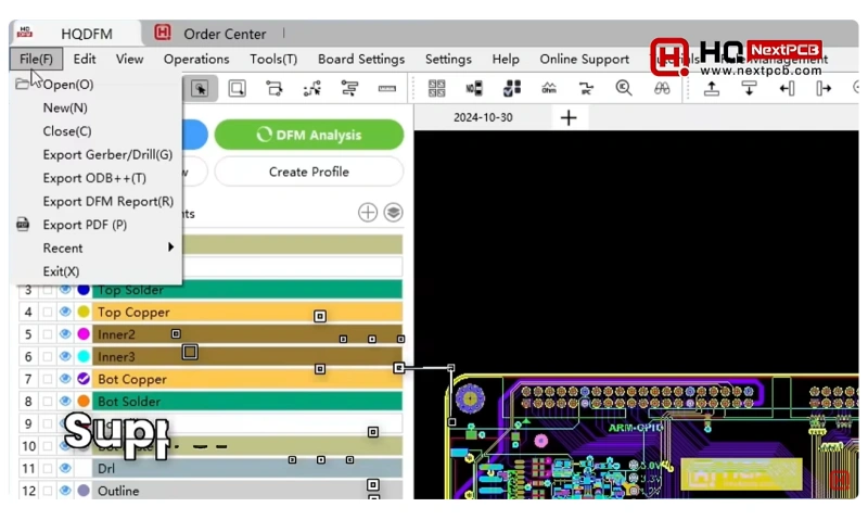
Layer Management: Clear Separation of Assembly and Fabrication Layers
Effective layer management is crucial for high-quality Assembly Drawings. The Assembly Drawing should utilize a separate Assembly Layer that includes only component outlines, Reference Designators, and polarity marks, free from the constraints of solder mask or pads. This is fundamentally different from the Silkscreen Layer. The silkscreen is the text and marking layer printed on the bare board, but DFM requirements mandate that silkscreen ink should not be printed over pads, vias, or underneath components, to prevent affecting soldering or obscuring critical markings.
Due to DFM requirements, silkscreen information on the bare board (such as RD or Pin 1 markings) is often clipped or removed where it conflicts with pads or solder mask openings, resulting in incomplete information. The independent Assembly Layer is key to compensating for this defect. It provides a complete, unclippled graphical representation of component outlines and orientation, serving as the unique and unambiguous reference standard for machine setup and manual operations.
Multi-View Strategy: Combining 2D and 3D Views
Traditional Assembly Drawings often rely on 2D top-down views to show component layout. However, for complex designs with strict mechanical constraints, a multi-view strategy is essential. In addition to top/bottom views, magnified detail views should be provided to clearly show high-density areas.
> Recommend reading: PCB Thermal Design Basics (2): Component Layout
Furthermore, the introduction of 3D Assembly Views has become a best practice. 3D visualization allows designers to more easily spot design issues like component spacing, height, and physical interference before actual production. The Assembly Drawing should be accompanied by 3D STEP files, allowing assembly and mechanical engineers to verify the final mechanical and thermal feasibility.
Data Consistency: Interlinking the Design Data Ecosystem
The accuracy of the Assembly Drawing relies heavily on interlinking mechanisms within the design data ecosystem. This means that component data in the Assembly Drawing must remain synchronized in real-time with the BOM, Pick & Place files, schematics, and 3D models. The industry encourages using automated tools for BOM integration and data synchronization, rather than relying on time-consuming and error-prone manual updating processes. Automated synchronization mechanisms ensure that the RD, part number, value, and footprint remain consistent across all documents, significantly reducing data conflicts.
Verification and Review Process: DFA/DFM Checks
A rigorous verification and review process must be conducted before the files are delivered to the manufacturer. This includes Design Review (DR) and Assembly Review (AR), ensuring the Assembly Drawing complies with the actual capabilities of the production line. The review checklist should cover verification of the integrity of the manufacturing data exports (Gerber/ODB++/IPC-2581), and checking the orientation of all polarized components.
It is important to note that Design Rule Checks (DRC) only verify rules set internally within the design tool, whereas Design for Manufacturing (DFM) focuses on assessing the design's compatibility with real-world manufacturing and assembly capabilities, including minimum pad spacing, thermal design, etc. Silkscreen should maintain minimum spacing from pads/vias/fiducials, avoiding coverage or obscuring critical markings, to prevent solderability and inspectability issues. The Assembly Drawing review is a crucial step in the DFM process, isolating potential production defects (such as upside-down or misplaced components) from the theoretical design.
IV. Error Types and Prevention: Practical Guide to Reducing PCBA Defects
The Assembly Drawing is the first line of defense against production defects. Understanding and avoiding common errors is essential for improving PCBA quality.

Component Orientation and Polarity Defects
Incorrect component orientation and polarity marking are among the primary causes of circuit board functional failure. Any deviation in the IC Pin 1 indicator, capacitor polarity, or diode direction can lead to the need for rework or outright scrapping of the board. Prevention strategies require using clear, IPC-A-610 compliant graphic symbols to denote polarity on the Assembly Drawing, and placing a strong emphasis on verifying all high-risk polarized components during the First Article Inspection (FAI).
Inconsistent Identifiers and BOM
The Reference Designator in the Assembly Drawing must perfectly match the name or footprint in the BOM or schematic. When names or footprints clash, it can lead to the procurement department ordering the wrong part, or assembly personnel installing the correct part in the wrong location or footprint. The key to prevention is adopting a unified data management platform, ensuring that the RD has uniqueness and consistency throughout the entire design lifecycle.
Visual Defects and Information Overlap
Visual defects include silkscreen overlapping pads or vias, which can not only cause soldering defects but also obstruct AOI or manual inspection. Furthermore, critical notes being obscured by component outlines or other graphics can lead to misinterpretation. Designers must ensure all critical information on the Assembly Drawing is placed in a clear, non-overlapping position.
Special Considerations for High-Speed/High-Frequency Circuits
For boards containing high-speed or high-frequency signals, the Assembly Drawing may require additional, performance-related notes. This could include strict routing requirements for critical impedance traces, or tight tolerance requirements for sensitive component placement. Adding a dedicated DFM notes section to the Assembly Drawing, listing these special requirements, prevents minor assembly deviations from affecting final signal integrity.
Lack of Change Records or Version Control
Using the wrong Assembly Drawing version during the production run is a major risk that leads to batch errors. The Assembly Drawing must include a clear version number, revision date, and a detailed summary of changes. All design changes should be managed through a formal Engineering Change Notice (ECN) process, ensuring the factory always uses the latest, verified file for production.
V. Advanced Design: HDI, Rigid-Flex, and 3D Assembly Views
As design complexity increases, Assembly Drawings must adapt to the challenges posed by emerging technologies.
Complex Structure Annotation in HDI and Miniaturization Designs
HDI and miniaturization designs (such as those using 01005 components) make precise component alignment and polarity marking extremely difficult. For these designs, the Assembly Drawing must provide high-magnification detail views, clearly showing the exact placement area, Pin 1 marking, and soldering area for tiny components. Additionally, since HDI boards typically feature complex blind/buried via structures, the Assembly Drawing should use supplemental side views or data models (like IPC-2581) to clearly convey stack-up and drilling information.
Rigid-Flex Boards: Special Assembly Annotation Methods
For rigid-flex boards, the Assembly Drawing must guide the board's three-dimensional final shape in addition to the standard component layout. Designers must clearly annotate the flexible regions with the bending radius, fold lines, and component keep-out zones on the Assembly Drawing.
In rigid-flex design, the Assembly Drawing guides not only initial component placement but also the final assembled form. High-quality Assembly Drawings require detailed mechanical assembly steps and 3D views to ensure that components or solder joints do not stress the flexible area when folded or bent, thus preventing fatigue cracking, which is vital for long-term product reliability.
3D Assembly Views and Three-Dimensional Placement Information
3D visualization is a powerful tool for solving complex mechanical constraints and assembly interference. Using 3D CAD models to supplement Assembly Drawings allows designers to spot issues like component spacing, height, and physical interference before production. For designs with tight enclosures or large mechanical parts (e.g., heat sinks, connectors), the Assembly Drawing should include 3D views or STEP files for final physical interference verification.
Smart Assembly Drawings: Integration with AOI/Vision Inspection Systems
Modern Assembly Drawings are moving toward an "intelligent" direction, meaning they directly provide structured data to automated inspection equipment. Automated Optical Inspection (AOI) systems require expected component X/Y position and rotation information as an input model. The intelligent Assembly Drawing should clearly label which components are critical inspection targets and which components (e.g. BGA, QFN) require inspection of hidden solder joints using Automated X-ray Inspection (AXI), thereby optimizing the machine's inspection path and parameter settings.
Electronic Design Automation (EDA) tools play a central role in generating Assembly Drawings. Mainstream tools like Altium Designer, KiCad, OrCAD, and PADS all support exporting PnP files and mechanical Assembly Drawings (typically in DXF/DWG/PDF format). However, achieving automation and zero-defect goals in PCBA manufacturing requires data formats to shift from traditional file groups to unified, intelligent data packages.
Next-Generation Output Formats: ODB++ and IPC-2581
ODB++ is a proprietary, hierarchical, compressed data format designed to simplify CAD to CAM data exchange. It can contain complete manufacturing and assembly information in a single file, including stack-up, BOM, component placement coordinates, part height, mounting style, and assembly surface (top/bottom) details. This format offers versatility across various phases of board manufacturing.
IPC-2581 is an open-standard XML format viewed as an alternative to ODB++. This format uses an XML structure, covering bare board fabrication, assembly manufacturing data, component, and test information in a single record, and supporting design/assembly variants. IPC-2581's power lies in integrating bare board fabrication data, stack-up information, electrical net information (netlist), and all required assembly data (BOM, coordinates, and rotation) into a single record. It even supports assembly information specific to different product variants.

These two formats serve as the cornerstone for achieving manufacturing automation. The inherent error rate of the traditional multi-file delivery model (AD + Gerber + BOM + PnP) stems from the difficulty of manually correlating and synchronizing files. ODB++ and IPC-2581 minimize this risk by enforcing data synchronization within a structured file, making them prerequisites for achieving Industry 4.0 automated production lines (such as lights-out SMT).
Table III: Digital Assembly File Format Comparison
|
Format
|
Primary Use
|
Includes Complete Assembly Data
|
Advantages
|
|
Gerber RS-274X
|
Bare Board Graphics Fabrication
|
No (Requires separate PnP, lacks stack-up/BOM)
|
Long-standing, highly universal, focuses on graphical geometry.
|
|
ODB++
|
CAD to CAM Data Exchange
|
Yes (Includes BOM, Coordinates, Stack-up)
|
Single compressed file with all manufacturing info, hierarchical data structure, easy CAM import.
|
|
IPC-2581
|
Universal Data Exchange Standard
|
Yes (Includes BOM, Coordinates, Stack-up, Assembly Variants)
|
Open XML standard, supports assembly variants, provides traceability.
|
Data Interface and Version Control
Data interface technology aims to ensure data synchronization. Component library data—such as footprint dimensions and Pin 1 location—must consistently align across the schematic, PCB layout, and Assembly Drawing output. In terms of documentation management, strict version control using PLM/PDM or systems like Altium 365 is critical to ensure the factory always uses the latest, approved version of the Assembly Drawing.
> Recommend reading: PCB Schematic vs PCB Layout

VII. Process Synergy: Assembly Drawings and Automated Production Lines
The value of the Assembly Drawing is realized through its deep synergy with the entire PCBA manufacturing process.

Intelligent Inspection: Assembly Drawing-Driven QC Process
In highly automated PCBA production lines, the Assembly Drawing's role is shifting from a "manual guidance document" to a "machine vision-driven model." The Assembly Drawing's quality directly dictates the speed and accuracy of automated inspection system setup.
-
AOI (Automated Optical Inspection): The AOI system captures high-definition images of the board and compares them against the expected component position (X / Y) and rotation information provided by the Assembly Drawing. AOI typically uses Centroid/XY (RefDes, X/Y, θ) to quickly generate programs, and often utilizes PnP/XY data to accelerate modeling, rapidly detecting defects like missing parts, misalignment, and wrong orientation.
-
SPI (Solder Paste Inspection): SPI directly measures solder paste volume/height/area/offset to control the quality of the printing process; the Assembly Drawing is not a direct data source for SPI programming, but data consistency and process tolerances indirectly influence stencil apertures and acceptance thresholds.
-
AXI (Automated X-ray Inspection): For bottom-terminated components like BGAs and QFNs, traditional optical inspection cannot check solder joints. The Assembly Drawing must clearly indicate the location of these components so that AXI, targeting BGA/QFN bottom-side solder joints, can detect defects like voids, bridging, and Head-in-Pillow (HiP), although the detection rate and false positive rate for HiP are influenced by machine type/algorithm/threshold.
Testing Phase: Assembly Drawing Value for ICT and Functional Testing
-
ICT (In-Circuit Testing): ICT uses a "bed-of-nails" fixture to contact test points or vias on the PCB via spring-loaded pogo pins, testing the electrical performance of each component and circuit path. The Assembly Drawing must clearly annotate the location, type, and clearance area of all test points, as this forms the basis of the fixture design.
-
FCT (Functional Testing): The AD helps test engineers quickly identify critical test components, interface locations, and net names for test points, accelerating the development and deployment of functional test systems.
Long-Term Support: Assembly Drawing Value in Repair, Rework, and Customer Service
The value of the Assembly Drawing increases over the product's lifecycle. After a board failure, repair engineers must rely on the AD and schematics to quickly locate the faulty component, confirm its correct orientation, and verify the replacement model. Lacking a high-quality Assembly Drawing or schematic may force repair personnel to spend significant time and effort reverse-engineering the circuit, greatly increasing Operational Expenditure (OpEx) and equipment downtime. Therefore, a high-quality Assembly Drawing is a critical asset for lowering long-term operating costs and boosting customer satisfaction.
VIII. Case Study: Optimizing Assembly Drawings in Complex Projects
Optimizing an Assembly Drawing lies in attention to detail and targeted preparation.
Example Breakdown: Double-Sided SMT + Through-Hole (THT) Mixed Technology Board
For mixed technology boards, the Assembly Drawing must clearly distinguish between components on the top and bottom layers. For through-hole components (THT), pin forming and soldering requirements should be specifically noted. The Assembly Drawing typically uses different colors or legends to differentiate SMT components (usually automatic placement) from THT components (often requiring manual or selective wave soldering), and guides the corresponding soldering sequence.
Detail Annotation Methods for High-Density Boards
In areas with BGA arrays, high-density connectors, or micro-components, where Reference Designator silkscreen may be compressed or removed, the Assembly Drawing must provide high-magnification detail views. These magnified views clearly show the Pin 1 location, the exact component outline, and its associated RD, ensuring operators do not misplace parts due to visual confusion.
Case Study: Using 3D Models/Views to Aid Assembly
In a compact industrial control module design, large heat sinks and complex connectors needed to be installed. The designer used 3D cross-sectional views to show the clearance between components and the heat sink, and annotated the torque requirements for critical screw holes. This 3D view prevented component collision issues that could not be discovered using 2D drawings alone, significantly reducing mechanical interference risks.
IX. Future Outlook: The Trend of Intelligent and Automated Assembly Drawings
The future development direction of the Assembly Drawing is deep intelligence and comprehensive integration with manufacturing systems.
Application of AI-Assisted Annotation/Suggestion Tools
The application of AI and machine learning tools is entering the Assembly Drawing generation field. By analyzing historical DFM rules, manufacturing capacity limits, and past rework data, AI can automatically generate context-relevant DFM notes, such as cleaning keep-out zones, special handling warnings for thermal components, or suggesting optimal placement for Reference Designators. Intelligent checking tools can automatically compare the consistency of AD, BOM, and PnP files, proactively catching RD or polarity conflicts caused by human oversight.
Industry 4.0 Vision: Assembly Drawing as the Input Data Source for Digital Twins
In the Industry 4.0 environment, Assembly Drawing data (especially structured ODB++ or IPC-2581 files) serves as a core input data source for digital factory simulation models. This data is used for virtual assembly, process optimization, and capacity prediction.
Future Assembly Drawings will no longer be static PDF or DWG files. They will be dynamic, scalable data models that can automatically update based on production variants or version changes, achieving instant synchronization from "design data to manufacturing process." This dynamic scalability is a key technology for realizing highly automated production lines.
Integration of Assembly Drawings with Sustainable Design/Green Electronics
With global focus on sustainability, Assembly Drawings may need to include annotations related to green electronics. This includes clearly identifying components made with special materials or high-value components that are easily disassembled/recycled, supporting future product circular economy requirements.
X. Conclusion and Recommendations
Reaffirming the Impact of AD Quality on PCBA Cost, Reliability, and Efficiency
The PCB Assembly Drawing is the bridge connecting design and manufacturing. The quality of the Assembly Drawing directly determines the efficiency of PCBA production, the rework rate, and the reliability of the final product. A high-quality Assembly Drawing is a prerequisite for achieving zero-defect production and shortening Time-to-Market. By adhering to standardized drafting specifications and adopting advanced digital data formats, the entire PCBA supply chain can be significantly optimized.
NextPCB's Advantages in High-Quality Assembly Data Handling and DFM Support
NextPCB is committed to providing professional-grade PCBA manufacturing services, with a particular emphasis on strict DFM review of customer-submitted data. NextPCB supports ODB++ and IPC-2581, advanced data formats for import and processing, ensuring design data is transferred seamlessly and accurately to automated production lines. Our professional DFM team assists customers with expert Assembly Drawing reviews before production, focusing on high-risk items like polarity, fiducials, and component spacing, eliminating design errors before they enter the workshop.
> Ready to transform your PCB design into a highly reliable product? Use our instant quote system and enjoy one-stop service for rapid prototyping and mass production, ensuring your product is delivered to the highest standards.
If you are evaluating manufacturing vendors for your next hardware spin, check out our comprehensive NextPCB vs JLCPCB vs PCBWay comparison guide.
Assembly Drawing Submission Checklist for Design Engineers
To ensure a smooth PCBA project, designers should strictly follow this checklist when submitting Assembly Drawings:
- 1. RD and BOM Consistency: Confirm that all Reference Designators in the Assembly Drawing match the BOM 100%, with no footprint conflicts.
- 2. Polarity and Orientation: Ensure that the direction markings for all polarized components (IC Pin 1, electrolytic capacitors, diodes) are clear, standardized graphically, and comply with IPC-A-610 standards, as per the current revision.
- 3. Fiducial Compliance: Confirm that at least three global fiducial marks are set, that they are solid circles, with a diameter between 1.0 mm and 3.0 mm, and that the fiducial area is clear of solder mask.
- 4. PnP File Synchronization: Confirm that the Pick & Place file has been provided, and its coordinate origin and units are consistent with the Assembly Drawing's definition.
- 5. Mechanical and 3D Views: If the design includes complex mechanical structures or tight spaces, confirm that 3D models or 3D views are provided for mechanical interference checks.
- 6. Detail Views: Confirm that magnified detail views are provided for high-density or micro-component areas.
- 7. Silkscreen and DFM: Confirm that the silkscreen layer design adheres to DFM specifications, avoiding ink printing over pads and vias to prevent impact on solderability.
Upcoming Articles / Series Preview
Stay tuned for our next professional article series: "From Gerber to IPC-2581: The Future of PCBA Data Formats."
Get an Instant Quote Now
About the Author
With extensive experience in the PCB and PCBA industry, Stacy has established herself as a professional and dedicated Key Account Manager with an outstanding reputation. She excels at deeply understanding client needs, delivering effective and high-quality communication. Renowned for her meticulousness and reliability, Stacy is skilled at resolving client issues and fully supporting their business objectives.


 NextPCB Capabilities
 PCB Assembly
 Layer Buildup
 SMD-Stencils
 PCB Design-Aid & Layout
 Mechanics
 Surface
 Quality
 Drills & Throughplating
 Factory & Certificate


