
 Surface


Lolly Zheng- Sales Account Manager at NextPCB.com

 NextPCB Capabilities
Printed Circuit Boards
NextPCB Capabilities
Printed Circuit Boards
 PCB Assembly
 Layer Buildup
 SMD-Stencils
 PCB Design-Aid & Layout
 Mechanics
 Quality
 Drills & Throughplating
 Factory & Certificate
 PCB Assembly Factory Show
Certificate
PCB Assembly Factory Show
Certificate
Support Team
Feedback:
support@nextpcb.com


Introduction
Editor's Note (February 2026): This article has been updated with the latest industry data regarding Ultra-HDI trends, AI hardware requirements, and manufacturing standards for the 2026-2027 production cycle.
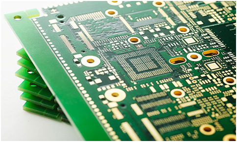
HDI (High-Density Interconnect Board) is a compact board designed for small-volume users. Compared to ordinary PCB, the most significant feature of HDI is the high density of wiring.
In the context of 2026 electronics manufacturing, HDI has become the backbone of "Edge AI" devices and foldable smartphones. As chips move toward 3nm and 2nm architectures, the demand for HDI boards that can support extreme miniaturization has surged.
The difference between HDI and standard PCBs is mainly reflected in the following 4 aspects:
HDI board uses the traditional double-sided board as the core board, formed through the continuous accumulation of laminated layers. This method of continuous layer accumulation is also known as the Build-up Multilayer (BUM) process. Compared to conventional boards, HDI boards have the distinct advantages of being "light, thin, short, and small".
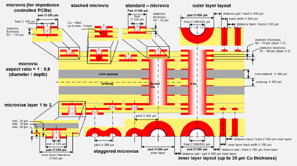
The electrical interconnection between the layers of the HDI board is achieved through conductive through-hole, buried via, and blind via connections. Unlike ordinary multilayer PCBs, HDI boards are designed with a large number of micro-buried blind vias.
Ordinary PCBs are usually drilled using mechanical methods, whereas HDI PCBs are drilled using laser technology. Consequently, the number of layers and the aspect ratio of HDI PCBs are often increased to accommodate complex designs.
The high density of HDI boards is mainly reflected in the hole, line, pad density, and interlayer thickness. As of 2026, the industry is shifting from standard HDI to Ultra-HDI (UHDI) to meet the needs of high-performance computing.
HDI PCBs not only facilitate miniaturized product designs but also meet higher standards of electronic performance and efficiency.
The increased interconnect density of HDI PCBs allows for enhanced signal strength and improved reliability. Furthermore, HDI boards offer better shielding against Radio Frequency Interference (RFI), Electromagnetic Interference (EMI), static discharge, and improve thermal conduction.
2026 Performance Note: With the adoption of PCIe 6.0 and early 6G prototyping, the signal integrity provided by HDI's shorter transmission paths (via micro-vias) is crucial for reducing signal loss and latency.
While HDI offers superior volume and electrical performance compared to ordinary PCBs, the manufacturing threshold and process difficulties are significantly higher. A critical area of focus is the buried plug holes.
The core pain point of HDI manufacturing is the buried plugging hole process. If not executed correctly, major quality issues arise, such as:
| Feature | HDI PCB | Traditional PCB |
|---|---|---|
| Layer Count | Typically 6-12 or more (High Layer Count) | Usually 2-4 layers |
| Via Types | Through-hole, Blind vias, Buried vias, Stacked vias | Primarily Through-hole vias |
| Line Width & Via Size | Finer lines (down to 30-75μm) and laser-drilled microvias | Larger lines and mechanically drilled vias |
| Functionality | Miniaturization, High performance, Design flexibility | Standard functionality |
| Manufacturing Complexity | High (Requires Laser drilling, Sequential Lamination) | Low to Medium |
| Cost | Higher initial cost (offset by reduced board size in 2026) | Lower initial cost |
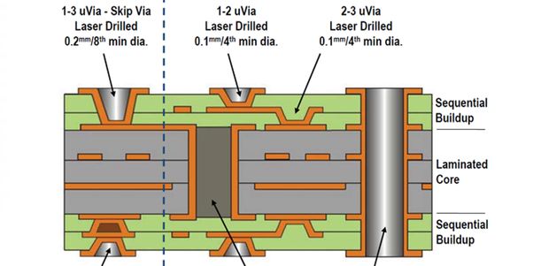
The stack-up of an HDI PCB is a critical blueprint that defines the arrangement and composition of its various layers. Here is a breakdown of the key components:
Surface Layers: Top and bottom layers provide connection points. In 2026 designs, "Pad-in-Via" technology is standard to maximize component density.
The fabrication of HDI PCBs is a complex process. Key differences include:
HDI PCBs are the backbone of modern electronics. Key application areas in the 2026 landscape include:
A: HDI PCBs offer significantly higher wiring density than ordinary PCBs. While standard boards have larger limits, HDI processes can currently produce fine traces with a width of 0.025 mm and spacing of 0.05 mm. Some advanced processes can even achieve trace widths as narrow as 12 μm.
A: Ordinary PCBs primarily use Plated Through-Holes (PTH). In contrast, HDI PCBs utilize microvias (blind and buried vias) with diameters smaller than 0.25 mm. These microvias allow for a "small, thin, dense, and flat" design, which is essential for modern compact electronics.
A: Standard PCBs are typically pressed once, whereas HDI PCBs use a sequential build-up (SBU) method.
A:
Not all board factories have the capability to manufacture high-reliability HDI boards. NextPCB has been refining this technology for over 15 years.
Today, NextPCB's HDI manufacturing utilizes a complete, in-house system with no outsourcing. We have invested heavily in advanced 2026-era equipment (such as Laser Direct Imaging and automated optical inspection). All quality acceptance standards strictly adhere to IPC-2/IPC-6012 Class 2 and Class 3 standards—ensuring hole copper thickness ≥ 20μm—to guarantee the high reliability required for modern high-tech applications.

Still, need help? Contact Us: support@nextpcb.com
Need a PCB or PCBA quote? Quote now

