
 Surface


Arya Li, Project Manager at NextPCB.com

 NextPCB Capabilities
Printed Circuit Boards
NextPCB Capabilities
Printed Circuit Boards
 PCB Assembly
 Layer Buildup
 SMD-Stencils
 PCB Design-Aid & Layout
 Mechanics
 Quality
 Drills & Throughplating
 Factory & Certificate
 PCB Assembly Factory Show
Certificate
PCB Assembly Factory Show
Certificate
Support Team
Feedback:
support@nextpcb.com


Introduction
Mixed-technology PCB assembly represents a sophisticated and strategic approach to modern electronics manufacturing, combining the high-density miniaturization of Surface-Mount Technology (SMT) with the mechanical robustness and power-handling capabilities of Through-Hole Technology (THT) on a single board. This guide provides an exhaustive analysis of mixed assembly, detailing its foundational principles, advanced manufacturing processes, critical Design for Manufacturability (DFM) rules, and a deep-dive into its economic and quality assurance drivers. The report will demonstrate that the choice to utilize mixed assembly is not a mere compromise but an intentional engineering decision that optimizes for performance, reliability, and cost-efficiency in complex, high-stakes applications across the automotive, medical, and aerospace sectors.
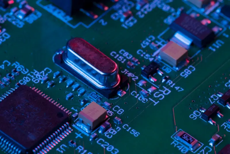
Table of Content:
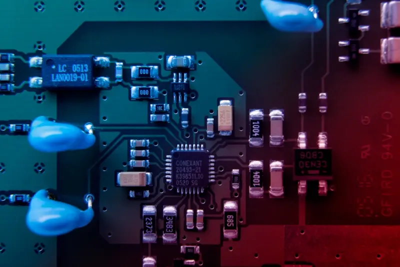
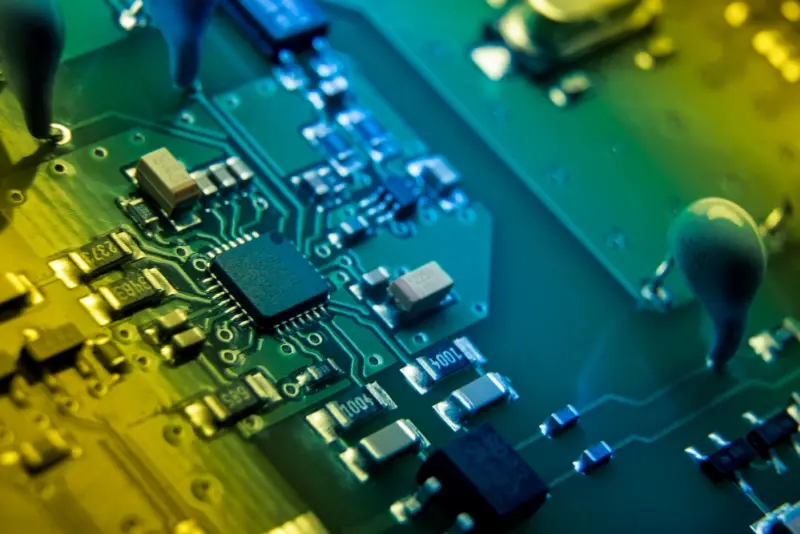
Mixed-technology PCB assembly is the manufacturing process of integrating both Surface-Mount Technology (SMT) and Through-Hole Technology (THT) components onto a single printed circuit board. By combining SMT's ultra-high component density with THT's superior mechanical durability, this hybrid approach delivers optimal signal integrity, thermal management, and physical robustness for complex, high-reliability applications. It allows designers to combine the strengths of each technology on a single board—SMT for compact, high-speed components and THT for mechanically secure parts such as connectors or large capacitors. Mixed assembly is a common requirement in applications where both performance and reliability are critical, including the industrial, medical, automotive, and defense sectors. The choice to use this technology enables greater design flexibility and supports a wider range of component types within a single build, while acknowledging that it adds a layer of complexity to the manufacturing process.
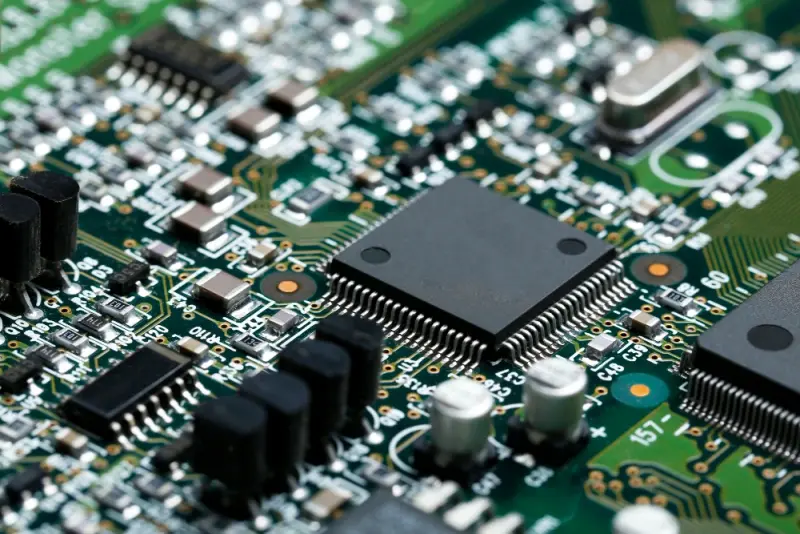
SMT is the dominant method for modern electronics due to its ability to create compact, high-performance circuits. In this process, tiny components with flat contacts are soldered directly onto pads on the board's surface. The assembly process involves three main stages: solder paste printing, where a stencil applies solder paste to the PCB's pads; automated pick-and-place, where machines precisely mount the components; and reflow soldering, where the board is heated to melt the paste and create a permanent joint.
This highly automated process offers several key advantages.
THT, a method that predates SMT, remains indispensable for applications where physical durability and high power are paramount. THT components have leads that pass through plated holes in the PCB and are soldered on the opposite side, typically by wave soldering or manual soldering. This method, while more labor-intensive and slower than SMT, creates an inherently robust mechanical bond that resists vibration, shear forces, and thermal stress.
The enduring advantages of THT are directly tied to its physical characteristics. The solder joint, which fills the plated hole and solders to both sides of the board, provides superior mechanical strength compared to a surface-level SMT joint. This makes THT ideal for heavy components like large electrolytic capacitors, high-current transformers, and connectors that are frequently plugged and unplugged. The larger physical size of THT components is also often better suited for dissipating heat, making them a preferred choice for high-power applications. However, a key disadvantage is that the long leads of THT components increase parasitic inductance, making them unsuitable for high-frequency, high-speed signal paths where signal integrity is a priority. Furthermore, the larger size of THT components facilitates manual handling, making this technology highly practical for low-volume prototyping, small-batch production, and in-field repairs.
A superficial comparison of SMT and THT suggests that SMT's speed, cost-efficiency, and compactness have made THT obsolete. However, a deeper analysis reveals that THT's continued relevance stems from its unique and irreplaceable strengths in mechanical robustness and thermal management. The physical size and leads of THT components, which are considered disadvantages in terms of density, are precisely what provide the mechanical and thermal benefits that SMT cannot replicate.
The rise of mixed assembly is a recognition of this dynamic. It represents a sophisticated, non-simplistic approach to design, where the choice is not which technology is superior, but which is best for a specific function. This hybrid strategy allows a single board to incorporate the best of both worlds, enabling designers to meet complex and often conflicting requirements—such as the need for both high-speed signal processing and high-stress connector durability—on a single, integrated platform.
The following table provides a detailed comparative matrix of SMT, THT, and Mixed Assembly, illustrating the strategic trade-offs inherent in each technology.
|
Metric |
SMT (Surface-Mount) |
THT (Through-Hole) |
Mixed Assembly |
|
Cost (High Volume) |
Lower (due to automation) |
Higher (labor, drilling) |
Moderate (leverages automation) |
|
Component Density |
Very High (100+ per in²) |
Low (20 per in²) |
High (combines SMT density with THT) |
|
Mechanical Strength |
Reliable for most uses |
Very High (robust joints) |
Very High (THT for high-stress parts) |
|
Assembly Speed |
Very Fast (automated pick-and-place) |
Slower (manual/insertion machines) |
Varies, typically between all-SMT and all-THT, depending on the degree of THT automation |
|
Rework/Repairability |
Challenging (small components) |
Easier (manual handling) |
Moderate (THT parts are easy to swap) |
|
Typical Applications |
Consumer, IoT, Mobile devices |
Industrial, Aerospace, Power Supplies |
Automotive, Medical, Defense, Complex industrial |
Mixed assembly is a powerful approach that directly addresses complex engineering challenges by leveraging the unique advantages of SMT and THT on a single board. The decision to use this hybrid approach is not a default choice but a direct response to a product's operating environment and functional requirements.
The primary benefit of mixed assembly is its ability to create a highly reliable and durable product. By using SMT for the dense, high-speed circuit and reserving THT for components that will endure mechanical stress—such as connectors, transformers, and large capacitors—the final product achieves a level of robustness and stress-tolerance that neither technology could provide alone. One source notes that mixed assembly delivers "all the benefits of both mounting technologies," resulting in a "robust PCB assembly" that is highly reliable for long-life applications.
This approach also grants designers unparalleled flexibility. It enables engineers to "mix and match" packages, selecting the most suitable component for each specific function regardless of its mounting format. This versatility is crucial for complex designs where a particular component, such as a high-power transformer, may only be available in a THT package, while the corresponding microcontroller is exclusively SMT. The result is an optimized board that is not limited by part availability or technology constraints, leading to improved electrical performance, better signal integrity, and enhanced thermal management.
Mixed assembly is the technology of choice in industries where both miniaturization and robustness are non-negotiable requirements. The use of mixed assembly in these fields is not arbitrary; it is a direct response to the demanding operational environments and critical functional requirements of the products.
In each of these cases, the design philosophy is driven by the application's unique, non-negotiable needs. A power supply board for an industrial control unit, for instance, requires the mechanical strength of THT for its large capacitors and connectors while using SMT for the smaller, less-stressed signal components. This demonstrates a clear causal relationship: the demanding and often conflicting requirements of mission-critical products necessitate the use of a technology that can satisfy all of them simultaneously.
A common point of confusion arises from the similar terminology of "mixed-technology" and "mixed-signal" PCBs. A mixed-technology PCB, as described in this report, combines SMT and THT components. A mixed-signal PCB, by contrast, integrates both analog and digital circuits on a single board. These are distinct concepts, yet they often coexist. For example, a medical device might use a dense SMT digital processor and sensitive SMT analog amplifiers (making it a mixed-signal board), while also incorporating a rugged THT connector for the power supply (making it a mixed-technology board). Understanding this distinction is crucial for a complete analysis of a board's design. The most complex and high-performance electronic systems are often a blend of both concepts, leveraging the best of each domain to achieve optimal performance, durability, and signal integrity.
The manufacturing of a mixed-technology PCB requires a meticulously planned, multi-stage process that accommodates both SMT and THT requirements. The standard workflow for a double-sided mixed-technology board is a prime example of how modern assembly lines manage this complexity.
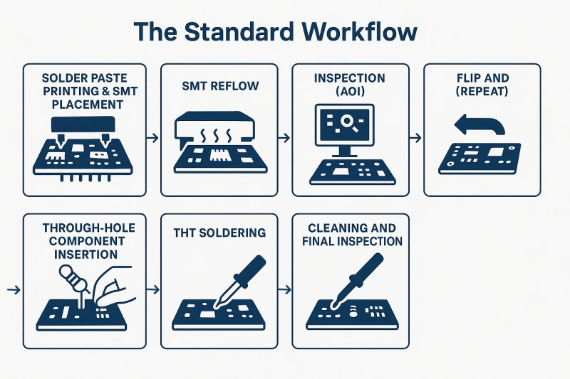
The assembly process is carefully sequenced to prevent damage to previously soldered components. The typical flow is as follows:
The choice of THT soldering method is a critical decision in mixed assembly. The board’s layout, specifically the proximity of SMT and THT components, directly dictates the optimal approach. The two primary methods are wave soldering and selective soldering.
The following table compares the two methods, highlighting how the board's design complexity and production volume drive the choice of soldering technology.
|
Metric |
Wave Soldering |
Selective Soldering |
|
Speed/Throughput |
High (hundreds of boards/hour) |
Slower (20-50 boards/hour) |
|
Cost |
Lower upfront cost, high-volume cost-effective |
Higher upfront cost, cost-effective for medium/small runs |
|
Precision |
Lower (can cause solder bridges) |
High (targets specific joints) |
|
Thermal Stress |
High (heats entire board) |
Low (only heats the joint) |
|
Ideal Use Case |
High-volume, simple THT boards |
Low-to-medium volume, complex mixed boards |
|
Typical Defect Rates |
Higher (due to solder splash/bridging) |
Lower (often under 1%) |
While SMT is inherently automated, the THT portion of the mixed assembly process has also seen significant advances in automation. The perception that THT is purely manual is outdated. Modern robotic insertion machines can place components with high speed and accuracy, reducing human error and optimizing labor costs. Specialized machines handle different component types, such as axial/radial components and irregularly shaped "odd-form" parts like connectors. These systems can achieve insertion rates of up to 4,000 components per hour, which significantly outpaces manual methods and makes mixed assembly viable for higher production volumes.
An increasingly common alternative for through-hole components is the "Pin-in-Paste" (PIP) or "Through-hole Reflow" process. This advanced technique allows through-hole components to be soldered using the same reflow oven as SMT components, eliminating the need for a separate wave soldering step. In this process, solder paste is applied to the through-hole pads, the components are inserted, and the board is then run through a standard SMT reflow oven. While highly efficient and capable of reducing production cycle times, this method is generally not a universal solution. It is best suited for small to medium batches or for specific components that can withstand the reflow temperature profile. For mission-critical applications requiring superior mechanical strength, such as in military or aerospace electronics, wave soldering or selective soldering is often still preferred due to their higher reliability.
For a mixed-technology PCB to be manufactured successfully and cost-effectively, the design must anticipate and solve potential manufacturing challenges before production begins. This discipline, known as Design for Manufacturability (DFM), translates the physical limitations of manufacturing equipment and processes into a set of actionable design rules.
> Recommend reading: New HQDFM V4.6 Release Now Supports KiCad
Proper spacing and clearance are not suggestions but are fundamental requirements for preventing manufacturing defects. The DFM rulebook serves as a direct translation of these physical constraints. For instance, maintaining a minimum of 0.2 mm spacing between SMT pads is essential to prevent solder bridging during reflow. Similarly, a clearance of at least 1.5 mm around PTH drill holes is necessary to accommodate soldering equipment and prevent thermal overlap with nearby SMT parts. Finally, a 3 mm edge clearance is recommended to prevent component damage during board handling and assembly. Adherence to these rules ensures that the design is not only functional but also manufacturable at scale.
The following table provides a prescriptive DFM checklist with specific, numerical rules and the rationale behind each.
> Recommend reading: Practical DFM Checklist and HQDFM Practice
|
Rule Type |
Parameter |
Recommended Value |
Rationale |
|
Component Spacing |
SMT Pad-to-Pad |
≥ 0.2 mm |
Prevents solder bridging during reflow soldering |
|
Component Clearance |
PTH Hole-to-SMT Pad |
≥ 1.5 mm |
Accommodates soldering equipment; prevents thermal overlap |
|
Board Clearance |
Component-to-Edge |
≥ 3 mm |
Prevents damage to components during handling and routing |
|
Via Placement |
Via-to-PTH Pad |
≥ 0.5 mm |
Prevents structural weakening of the board |
|
Component Grouping |
SMT Grouping |
Group components together |
Streamlines pick-and-place process and improves efficiency |
The combination of heat-generating THT components and densely packed, sensitive SMT components presents a significant thermal management challenge. DFM principles provide a clear roadmap for addressing this. Designers should use thermal vias with a diameter of 0.3-0.5 mm to dissipate heat to internal copper layers. The efficiency of this heat dissipation can be enhanced by increasing the number of thermal vias and using thicker inner copper layers (e.g., 2 oz/ft² or 3 oz/ft²), which can lower temperature rise by 10-20°C. Additionally, heat-generating components should be placed away from sensitive SMT parts, and heat sinks should be considered for any component with power dissipation exceeding 2 W.
In complex mixed-signal designs, the physical layout and layer stackup of the PCB can significantly impact electrical performance. Advanced mixed-technology boards often require careful impedance planning alongside component placement. Research indicates that customized 4-layer to 20-layer stackups are frequently utilized for high-reliability mixed-technology designs. Dedicating specific inner layers to ground and power planes—and pairing them with strictly calculated impedance control stackups—is a best practice for reducing EMI noise and preserving signal integrity, especially when high-frequency SMT circuits operate adjacent to high-power THT components.
These planes provide stable voltage and ground references, which are essential for preventing signal interference and crosstalk. The strategic placement of components and the use of dedicated planes ensures that both the compact SMT circuits and the high-current THT components can operate effectively without compromising performance.
A comprehensive understanding of mixed assembly requires an analysis of its economic profile and the critical quality assurance methods needed to ensure a reliable final product.
Mixed assembly is often perceived as more expensive than SMT-only builds due to the added process steps and complexity. However, a detailed economic analysis reveals a more nuanced cost curve. While the initial setup costs for a mixed assembly run may be higher than for a simple SMT build, these fixed costs are quickly amortized over a large production volume. The strategic use of automation for the SMT portion of the build, which accounts for the majority of components, significantly mitigates labor costs and boosts production efficiency. This approach makes mixed assembly a "very economical" solution for complex boards in large batches by avoiding unnecessary manual work and leveraging the speed of automated processes.
The economic decision for mixed assembly is a sophisticated calculation that considers the non-linear relationship between volume, board complexity, and technology mix. It is an investment in product durability and performance that can become highly cost-effective at scale. The cost per unit of a mixed assembly board can vary significantly, ranging from approximately $150 to $1,500 per panel depending on the percentage of each technology used. It's important to note that this wide cost range is for panel-level assembly of complex industrial, aerospace, and medical PCBs, with costs for simpler consumer electronics being much lower. This is a result of the careful balance between the low-cost, high-volume SMT portion and the more labor-intensive THT portion.
Just as the assembly process is a hybrid of two technologies, so too must the inspection process be. For a truly reliable product, a combination of inspection methods is required to catch both visible and hidden defects.
A modern, high-reliability assembly line will use a hybrid inspection model, deploying AOI for a quick, full scan of the board and reserving AXI for a critical sample of boards to verify the quality of hidden joints. This approach ensures comprehensive quality control and is a necessary investment in the production of complex, mixed-technology boards.
Q1: For a small production run (under 500 boards), is it cheaper to redesign my board for all-SMT or stick with mixed assembly?
Q2: Can I run through-hole components through an SMT reflow oven to save time?
Q3: Does mixing SMT and THT components negatively affect high-frequency signal integrity?
Q4: How do manufacturers prevent SMT components on the bottom layer from falling off during wave soldering?
Q5: What is the typical defect rate difference between wave soldering and selective soldering for mixed boards?
At NextPCB, we understand that mixed-technology PCB assembly is more than just a process—it's a strategic solution for complex, high-reliability applications. From automotive and medical devices to aerospace and defense systems, the ability to combine the miniaturization and efficiency of SMT with the mechanical strength of THT is a non-negotiable requirement for optimal performance.
Our expertise lies in turning this complex challenge into a streamlined, single-process solution for our clients. We seamlessly integrate SMT and through-hole assembly in one run, eliminating unnecessary steps and ensuring consistency from prototyping to full production. Our commitment to advanced manufacturing means we utilize automated robotic insertion for THT components and employ a hybrid inspection model, combining the speed of AOI for surface defects with the precision of AXI for hidden joints. This ensures every board meets the highest standards of quality and durability.
The future of electronics demands partners who are at the forefront of this technology. NextPCB continues to invest in state-of-the-art automation and intelligent inspection systems, allowing us to build the most complex and robust mixed-technology PCBs with exceptional speed and precision. For companies seeking a partner to realize their most demanding designs, our capabilities provide a complete, end-to-end solution.
Upload Your File & Get an Instant Quote
> Recommend reading: PCB Assembly - The Most Comprehensive Guide | NextPCB

Still, need help? Contact Us: support@nextpcb.com
Need a PCB or PCBA quote? Quote now

