Table of Contents
- Establishing the Manufacturing Framework and Quality Specification
- SMT Component DFM: Passives and Polarity Management
- Advanced High-Density Packages
- Mixed Technology and Mechanical Component Robustness
- Validation and Quality Inspection Protocols
- Design for Testability (DFT) Requirements
- Specialized Component DFM: High-Frequency Devices
- Expert DFM Recommendations Summary
- Translating Design into Manufacturing
I. Establishing the Manufacturing Framework and Quality Specification
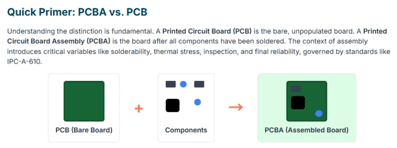
1.1. Quick Primer: PCBA vs. PCB (Why Assembly Context Changes Everything)
The Printed Circuit Board (PCB) serves as the foundation of an electronic circuit, the bare board produced through fabrication processes like etching, drilling, and applying protective layers. The PCB itself carries no active function. The Printed Circuit Board Assembly (PCBA) is the realized circuit function, where all PCBA electronic components (resistors, ICs, connectors) have been mounted and soldered onto the PCB. The PCBA stage involves automated PCBA component placement, soldering (reflow or wave soldering), and quality testing. Understanding this sequence is crucial: PCBA reliability is constrained by decisions made during the bare PCB design.
1.2. IPC Standards: Governing Quality and Consistency
Industry consistency, reliability, and manufacturability depend on adherence to standards published by the IPC (Association Connecting Electronics Industries). These standards are widely adopted in industry practice and are often specified by OEM/EMS contracts and quality systems as acceptance criteria or design basis.
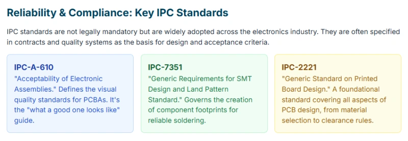
IPC-7351: Surface Mount Design and Land Pattern Standard
This standard is fundamental to Design for Manufacturability (DFM). It dictates the specific land pattern dimensions (footprints) for Surface Mount Devices (SMD) to optimize their behavior during automated assembly processes. Compliance ensures compatibility with standard manufacturing processes and guarantees reliable solder joints with proper toe, heel, and side fillets, actively preventing defects like tombstoning or solder bridging during reflow. This standardized geometry ensures predictable wetting and placement accuracy in high-precision pick-and-place and reflow systems. This predictability directly increases First Pass Yield, thereby minimizing rework, scrap, and operational costs. Thus, the economic function of IPC-7351 lies not only in reliability but also in promoting manufacturing predictability through standardization.
> New HQDFM V4.6 Release Now Supports KiCad

IPC-A-610: Acceptability of Electronic Assemblies
This document defines the ultimate quality benchmark. It outlines the acceptance criteria against which quality assurance and inspection are performed, categorized by the product's intended reliability class. Compliance dictates the acceptable quality of solder joints, component placement, and rework standards.
Table 1: IPC-A-610 Quality Classes and Reliability Requirements
|
Class
|
Description
|
Reliability Requirement
|
Typical Applications
|
|
Class 1
|
General Electronic Products
|
Functionality is the primary goal; short operating life expected.
|
Disposable devices, novelty electronics, promotional products.
|
|
Class 2
|
Dedicated Service Electronic Products
|
Extended life and continued performance required; minor cosmetic flaws acceptable.
|
Home entertainment systems, consumer computing devices (laptops), industrial monitoring.
|
|
Class 3
|
High Reliability/Critical Systems
|
Must perform continuously; failure is intolerable (e.g., life support, mission-critical).
|
Aerospace, medical implants, critical communication infrastructure.
|
> Recommend reading: IPC Class 2 vs 3: The Differences in PCB IPC Standards
II. SMT Component DFM: Passives and Polarity Management
The vast majority of components on a PCBA are passive Surface Mount Devices (SMDs), such as chip resistors and capacitors. Their small sizes make them highly susceptible to assembly defects.
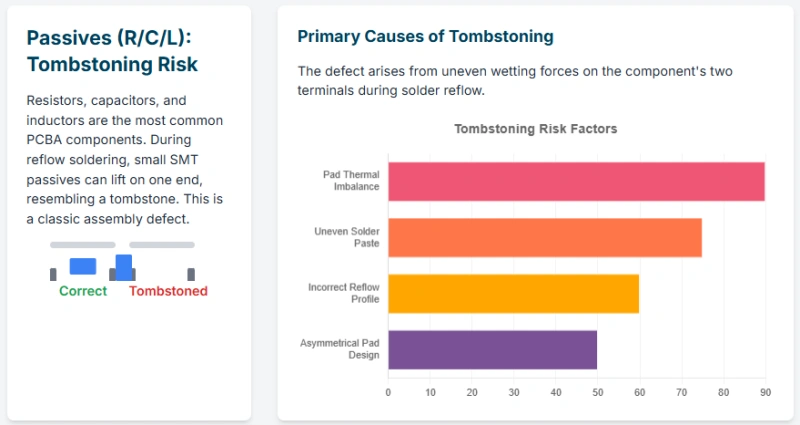
2.1. Passives (R/C/L): Packages and Tombstoning Risk
Tombstoning (where the component stands on one end) is a common failure mode that predominantly affects small two-terminal passive components (like 0402, 0603 packages).

Failure Mechanism
Tombstoning occurs during reflow soldering: as the molten solder on one pad wets the component lead and exerts a pulling force, the resulting asymmetrical surface tension can lift the low-mass component vertically if the solder on the opposing pad has not yet melted and wetted. This demands strict control over the symmetry of heat application.
Root Causes
- 1. Thermal Mass Difference: If one component pad is connected directly to a large copper plane (ground or power), that plane acts as a heat sink, causing the associated solder to heat up slower and delay wetting.
- 2. Pad or Paste Asymmetry: Unequal pad sizes or uneven solder paste deposition (e.g., poor stencil alignment) results in different solder volumes or thermal characteristics between the two pads, accelerating wetting on one side.
DFM Mitigation Strategies
- Symmetrical Footprints: IPC-7351 guidelines on pad size and spacing must be followed. Both pads must be identical in size and shape to ensure uniform heat transfer and wetting characteristics.
- Thermal Relief Design: When a component pad connects to a large copper area, it must be managed via thermal reliefs. Radial connections (e.g., 0.2 mm wide spokes) should be used to thermally isolate the pad while maintaining electrical connection. This practice minimizes the heat-sinking effect and ensures simultaneous melting on both sides. > Fundamentals of PCB Thermal Design | NextPCB
- Trace Balancing: If traces connect to the pads, they must have the same width and symmetric routing to maintain thermal equilibrium. The necessity of using thermal reliefs (spokes) on passive component pads inevitably adds slightly more impedance and path resistance than a solid, full copper connection. However, this DFM requirement prevents a mechanical defect (tombstoning), necessitating a small sacrifice of theoretical electrical perfection (impedance control) for practical high yield.
If you are evaluating manufacturing vendors for your next hardware spin, check out our comprehensive NextPCB vs JLCPCB vs PCBWay comparison guide.
2.2. Diodes & LEDs: Polarity Management and Orientation
Diodes, LEDs, and TVS diodes are polarized components that allow current flow in only one direction (anode to cathode). Incorrect orientation will render the circuit non-functional.
Silkscreen Requirements for AOI
To support both manual assembly and Automated Optical Inspection (AOI), clear and unambiguous polarity markings must be provided on the silkscreen layer.
Best Practice Markings
The recommended practice is to mark the cathode (negative terminal). Clear options include the schematic diode symbol, a simple straight line marking the cathode end, or the letter 'K' (to denote cathode, avoiding confusion with the 'C' for capacitors).
Ambiguous Markings to Avoid
Using only the '+' or '-' symbols can be ambiguous and is therefore not recommended:
For some devices (e.g., TVS diodes), the circuit potential may not align intuitively with the component's internal polarity (e.g., cathode connected to a positive rail). This ambiguity increases the risk of misplacement by assembly operators and can confuse automated inspection systems.
III. Advanced High-Density Packages: Thermal and Electrical Management
Complex packages characterized by hidden solder joints and high thermal requirements necessitate specialized design and assembly solutions.
3.1. Quad Flat No-Lead (QFN) Assembly Requirements
QFN packages utilize exposed thermal pads, requiring precise solder paste control to manage heat and prevent defects.
Thermal Pad and Via Array
The large exposed pad beneath the QFN is crucial for thermal management, relying on an array of thermal vias to conduct heat vertically to internal ground or power planes.
Solder Void Control
Voids (air pockets) in the thermal pad solder joint severely degrade thermal conductivity, leading to localized overheating.
Stencil Aperture Optimization
To control solder volume and reduce the risk of voids and surrounding pin bridging, the stencil aperture for the thermal pad must be reduced. DFM standards typically require reducing the printed solder paste area by 20% to 50% to ensure an appropriate volume of paste deposition.
- Pattern Implementation: This reduction is achieved by using window-pane or cross-hatching patterns that segment the paste deposition into smaller, evenly distributed blocks.
- Via-in-Pad Consideration: If thermal vias are placed directly in the pad, they must be monitored. If vias are large (e.g., >0.3 mm) and unfilled, molten solder can wick down the barrel during reflow, resulting in solder loss, insufficient joint formation, and potential protrusion on the underside of the PCBA.
> Check PCB Assembly Capabilities at NextPCB | Quick-Turn Prototype to Volume Production
3.2. Ball Grid Array (BGA) and Complex Integrated Circuits
BGAs are critical high-density ICs that rely on solder balls for connection. Their fine pitch necessitates the use of Via-in-Pad (V-I-P) technology for efficient routing.
Application of Via-in-Pad (V-I-P)
V-I-P places a plated hole (via) directly inside the component's solder pad. This technique is essential for routing fine-pitch BGA breakouts (HDI boards).
V-I-P Manufacturing Complexity: Fill and Planarization
V-I-P introduces significant cost and process complexity because the vias must be filled and planarized (capped and plated over).
- Purpose of Fill: The conductive layer of the pad requires a flat, uniform surface for solder paste application and reflow. Non-conductive epoxy fill and planarization prevent molten solder from wicking down the via barrel during reflow, ensuring adequate solder volume remains on the pad surface to form a reliable spherical solder joint.
- Cost Impact: The required filling and planarization significantly increase the complexity and cost of the PCB manufacturing process, as it involves additional process steps and specialized materials.
Table 4: Via-in-Pad Process Decisions and Cost Impact
|
Via Application
|
Fill/Planarization Required
|
Primary DFM Benefit
|
Cost Impact vs. Standard Vias
|
|
Signal/Escape Routing (BGA/QFN)
|
Requires non-conductive epoxy fill and planarization
|
High-density routing, smaller form factor, better signal integrity
|
High (significantly increased process complexity and cost)
|
|
Thermal Vias (QFN exposed pad)
|
Generally no fill required for heat dissipation
|
Superior thermal management and heat spreading
|
Moderate (may require complex array design)
|
Economic Justification
V-I-P is justifiable in compact, high-performance applications (e.g., smartphones, high-speed servers) where the space saved, improved signal integrity, and superior thermal performance outweigh the significantly increased cost. While V-I-P increases upfront Non-Recurring Engineering (NRE) costs and process steps, the competitive advantage gained from miniaturization often offsets the manufacturing increment cost over high-volume production runs. For low-volume prototyping, however, the complexity and NRE of V-I-P can make it prohibitively expensive.
> Recommend reading: Wearable Electronic Components: From Trackers to Wrist-Worn Micro-Computers
IV. Mixed Technology and Mechanical PCBA Component Robustness
While SMT dominates for density, Through-Hole Technology (THT) remains essential for high mechanical or power requirements, demanding sophisticated mixed-technology assembly strategies.
4.1. Through-Hole Technology (THT) for High Mechanical Stress
THT components are mounted using drilled holes (PTH or NPTH) and soldered on the reverse side, providing superior durability compared to SMT.
When THT is Mandatory
THT is used for components subjected to high physical stress or manual handling, such as connectors, relays, and large electrolytic capacitors. This robustness is why THT remains critical in industrial, defense, and aerospace applications.
Mechanical Reinforcement
For high-stress connectors, the design should include not only electrical THT pins but also dedicated THT mounting pegs or flanges to maximize the physical connection strength against shear forces and vibration.
4.2. DFM for Wave Soldering in Mixed Designs
Mixed boards (where SMT components are reflowed first, and THT components are added later) require either wave soldering (for all THT) or selective soldering (for specific THT groups).
Wave Soldering Shadowing Effect
In wave soldering, the board passes over a wave of molten solder. Improperly placed components can block the solder flow, creating a "shadow" effect that results in insufficient solder coverage on downstream pads, leading to weak or open joints.
Mitigation Through Orientation
Designers must orient THT components, especially long or wide packages, perpendicular to the established direction of the solder wave to ensure the solder contacts all leads uniformly. This requires communicating with the Contract Manufacturer (CM) about their assembly line orientation early in the design phase. When designing mixed boards, THT component placement is optimized not for electrical routing but to minimize the risk of shadowing during the wave soldering phase. THT component placement DFM rules are thus primarily dictated by the CM’s wave soldering machine setup, rather than tight routing requirements.
V. Validation and Quality Inspection Protocols
Verifying the assembly requires complementary inspection techniques capable of checking both surface placement (AOI) and internal solder joint quality (AXI).
5.1. Assembly Inspection Strategy (AOI vs. AXI)
- Automated Optical Inspection (AOI): AOI uses visible light to rapidly scan the PCBA surface. AOI systems are generally faster and more economical. They are suited for quickly detecting defects including component presence, orientation, polarity, component shift, and surface flaws like solder bridging.
- Automated X-ray Inspection (AXI): AXI uses X-rays to penetrate components and internal layers. AXI is typically slower and has lower throughput, but it is mandatory for hidden solder joints, such as BGAs, QFN thermal pads, and flip chips. AXI detects internal flaws like solder voids, insufficient solder, and hidden shorts. Data gathered by AXI regarding high voiding rates indicates deficiencies earlier in the line, particularly with stencil aperture design (QFN) or reflow profile optimization (BGA).
- Hybrid Approach: For IPC Class 3 products, manufacturers often adopt a hybrid strategy: AOI for fast, 100% surface inspection, and AXI for 100% inspection of critical packages or for sampling internal quality verification. AXI is not just a scrap mechanism but a critical process control tool.

5.2. Non-Destructive Inspection of BGAs (X-Ray Analysis)
The reliability of a BGA depends on the quality of its solder balls, which can only be assessed non-destructively via AXI.
BGA Acceptance Criteria (IPC-A-610)
IPC defines general acceptance based on smooth solder joints, clear boundaries, and consistent size/grayscale. Voids, however, are the primary challenge.
Void Control Targets
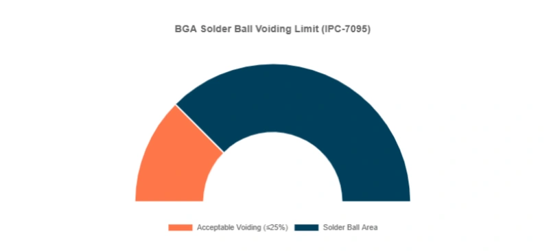
While BGA voids are not always directly linked to immediate failure, they significantly impact the thermal conduction path and joint lifespan. According to standards like IPC-A-610/IPC-7095, for voids within the solder ball, the common control limit is ≤25% of the area; some high-reliability applications or customer specifications may be stricter, though some applications might allow relaxation up to 30%.
- Criticality of Void Location: In some cases, the physical location of the void is more important than the overall percentage. Voids near the pad edge or in the fillet area are of particular concern as they create stress concentration points, increasing the likelihood of crack propagation during thermal cycling. Voids near the center of the pad are generally more tolerated.
Table 3: BGA Solder Joint Acceptance Criteria (IPC Derived)
|
Defect/Criteria
|
Inspection Method
|
Acceptance (High Reliability/IPC Class 3)
|
Significance
|
|
Solder Voiding
|
Automated X-ray Inspection (AXI)
|
Common control limit is ≤25% (customer specs may be stricter)
|
Excessive voids reduce thermal conductivity and structural integrity.
|
|
Void Location
|
AXI Analysis
|
Voids must be centrally located; voids near the pad edge/fillet are critical defects
|
Edge voids increase risk of crack propagation under shear stress.
|
|
Displacement/Twist
|
AXI/AOI
|
Offset relative to the pad must not exceed 25%
|
Ensures electrical connection and structural robustness.
|
VI. Design for Testability (DFT) Requirements
DFT ensures the finished PCBA can be quickly and reliably tested for opens, shorts, component values, and functional defects.
6.1. Choosing Electrical Test Method: ICT vs. Flying Probe
The decision to use In-Circuit Test (ICT) or Flying Probe Test (FPT) influences cost, throughput, and physical layout constraints.
- In-Circuit Test (ICT): ICT uses a "bed-of-nails" fixture to access all designated test nodes simultaneously. It is the fastest and most reliable method for detecting manufacturing defects in high-volume production due to its simultaneous node access. However, ICT requires significant upfront NRE investment for fixture creation.
- Flying Probe Test (FPT): FPT requires no fixture, using robotic probes to contact test points sequentially. FPT is more flexible, easily adapting to design changes, and is suitable for prototypes and low-to-medium volume production. The drawback is that the test time is slower than ICT.
6.2. DFT Implementation Guidelines
Testing point geometry varies by testing strategy.
ICT DFM Guidelines
ICT requires robust, widely spaced pads for reliable contact using standard 100 mil probes. ICT best practices commonly use a 0.035” (0.89 mm) test pad diameter**, with a minimum center-to-center spacing often set at 0.070” (1.78 mm)** ; for maximum repeatability and cost-efficiency, 0.100” (100 mil) standard probe spacing is recommended.
Flying Probe Test DFM Guidelines
FPT probes are more flexible and can target smaller features. Pad diameter and spacing can reach the 10–20 mil range, depending on the precision of the test equipment.
Table 2: Comparison of DFT Requirements by Test Method
|
Parameter
|
Flying Probe Test (FPT)
|
In-Circuit Test (ICT) (High Volume)
|
|
Applicable Volume
|
Prototype, Low-to-Medium Volume
|
High-Volume Mass Production
|
|
NRE/Fixture Cost
|
Low (No fixture required)
|
High (Fixed bed-of-nails)
|
|
Minimum Test Pad Diameter
|
10–20 mil range
|
0.035” (0.89 mm) common practice
|
|
Recommended Spacing (C-T-C)
|
16 mil (0.4 mm) minimum
|
0.070” (1.78 mm) common practice
|
|
Throughput
|
Slower (Sequential probing)
|
Fastest (Simultaneous probing)
|
Keepout Area Rules
Designers must ensure that tall components (often defined as components exceeding 6 mm in height) do not obstruct the flying probe's path.
- Target Selection: Preferred FPT targets are dedicated test pads or vias without solder mask. Probing directly on component leads or the solder fillet area should be avoided, as probe pressure can temporarily correct a false open joint, leading to a missed defect.
The demand for compact products often directly conflicts with the need for high-speed, reliable testing. Maximum component density requires fine-pitch routing, which necessitates smaller test pads and tighter spacing. This inevitably forces the use of the slower FPT method. Therefore, achieving maximum throughput (ICT) requires a compromise on board density (accommodating large pads and wide spacing). DFT must be planned before layout to prevent manufacturing bottlenecks.
Table 5: Flying Probe Test Keepout DFM Guidelines
|
Test Point Element (FPT)
|
DFM Rule/Dimension
|
Basis
|
|
Minimum Pad Diameter
|
10 mil (0.254 mm)
|
Minimum size for reliable probe contact repeatability.
|
|
Recommended Spacing (C-T-C)
|
16 mil (0.4 mm)
|
Limitation of physical probe tip size and movement capability.
|
VII. Specialized Component DFM: High-Frequency Devices
Reliable assembly of high-frequency circuitry requires treating the physical layout as an integrated electrical component, especially for crystal oscillators.
7.1 Crystal Oscillator Circuit Layout and Performance
Quartz crystals are used to generate precise clock signals, but their oscillation frequency is highly sensitive to the surrounding PCB environment.
Load Capacitance Dependency
The actual oscillation frequency is controlled by the effective load capacitance (CL) seen by the crystal. CL is determined by the external discrete capacitors (CL1,CL2) and the parasitic stray capacitance (CS) contributed by the PCB traces and planes.
Frequency Tuning and DFM
Since CS varies significantly with layout geometry (trace width, length, proximity to ground planes), the discrete load capacitor values must be optimized for each new board design to hit the nominal frequency.
- Post-Assembly Tuning: If testing reveals a higher-than-required frequency, the external capacitance must be increased; if the frequency is lower than required, the external capacitance must be decreased.
Symmetry Requirements
The layout around the crystal circuit must be strictly symmetric in terms of routing and component placement to ensure both crystal terminals see the same parasitic capacitance. Symmetric routing maintains the necessary negative resistance parameters for the oscillator circuit, which is crucial for reliable startup and long-term frequency stability.
Unlike low-frequency circuitry, the physical size and symmetry of the crystal layout are not merely mechanical considerations; they are an inherent part of the electrical component value (contributing to CS). Crystal frequency accuracy is highly dependent on CL, which is sensitive to layout-dependent stray capacitance (CS). Thus, layout deviations translate directly into frequency errors, potentially necessitating post-assembly adjustment of passive component values. This demonstrates how assembly inspection for high-frequency circuitry extends into electrical functional testing guided by DFM principles.
VIII. Expert DFM Recommendations Summary
High-yield, high-reliability PCBA manufacturing is achieved by integrating design and assembly constraints throughout the development cycle.
- 1. Standardization: Use IPC-7351 land patterns as the baseline for all SMT components to ensure compatibility with automated placement and reflow processes.
- 2. Thermal Symmetry: Universally apply thermal reliefs (spokes) on passive components connected to large copper planes to prevent tombstoning. Symmetrically match trace widths and pad geometry.
- 3. Density Management (V-I-P): Recognize that fine-pitch routing (BGA breakout) forces the use of via-in-pad, which requires non-conductive fill and planarization, significantly increasing cost and complexity. This cost increase must be justified by corresponding density or performance benefits.
- 4. Inspection Mandate: Determine the inspection methodology early. Use AOI for fast, surface checks, and mandate AXI for all hidden solder joints (BGA, QFN), applying acceptance criteria such as the ≤25% maximum void area limit for critical products (IPC Class 3).
- 5. Testability: Design for Testability (DFT) by reserving adequate space for test access. If high throughput (ICT) is required, pad diameter (e.g., 0.035") and spacing (e.g., 0.070") requirements must be met, accepting the resultant circuit board density constraints.
- 6. Polarity Control: Use clear, unambiguous silkscreen markings (K or straight lines) to denote polarity, and avoid using the ambiguous '+' or '-' symbols.
IX. Translating Design into Manufacturing: Choosing a Turnkey PCBA Partner
Translating an excellent theoretical design into a high-yield, high-reliability PCBA requires a manufacturing partner with the specialized capability to handle complex DFM and testing challenges.
NextPCB offers a one-stop turnkey PCBA service from prototype to high volume. We specialize in mastering the complex DFM challenges discussed herein, ensuring your products meet stringent industry standards:
- Advanced Assembly and Package Capabilities: NextPCB supports ultra-miniature 01005/0402 passive components, 0.25mm fine-pitch BGA, QFN, and other advanced packages, offering SMT, THT, and mixed-technology (reflow and wave soldering) assembly.
- In-Depth Inspection and Quality Assurance: Equipped with AXI (Automated X-ray Inspection), for BGA solder joint quality assurance, maintaining void control under 25%. We also offer comprehensive testing platforms including AOI, Flying Probe Test (FPT, no pad count limits), and In-Circuit Test (ICT, supporting up to 14,000 test points) as per NextPCB's manufacturing capabilities, ensuring compliance with IPC-A-610 Class II/III quality requirements.
- Design Optimization Support: Before production begins, NextPCB offers a complimentary DFM/DFA (Design for Manufacturing/Assembly) review service to help you optimize land patterns, crystal layouts, and proactively mitigate assembly defects like tombstoning or wave soldering shadowing, maximizing first pass yield.
Turn Your Design into a Flawlessly Assembled PCBA
- Ready to move from design to reality?
- NextPCB offers expert DFM checks and advanced assembly services to ensure your components perform exactly as intended.
- Our automated systems and rigorous inspection processes guarantee quality and reliability for prototypes and production runs.


 NextPCB Capabilities
 PCB Assembly
 Layer Buildup
 SMD-Stencils
 PCB Design-Aid & Layout
 Mechanics
 Surface
 Quality
 Drills & Throughplating
 Factory & Certificate