
 Surface


Stacy Lu

 NextPCB Capabilities
Printed Circuit Boards
NextPCB Capabilities
Printed Circuit Boards
 PCB Assembly
 Layer Buildup
 SMD-Stencils
 PCB Design-Aid & Layout
 Mechanics
 Quality
 Drills & Throughplating
 Factory & Certificate
 PCB Assembly Factory Show
Certificate
PCB Assembly Factory Show
Certificate
Support Team
Feedback:
support@nextpcb.com


A PCB schematic is a two-dimensional document representing the connectivity between two components mounted together or on the two sides of the circuit board. Or in simple words, a schematic represents the continuity of a signal path. A PCB schematic does not have anything to do with the placement of the components, the direction and length of the signal tracks, and the arrangement of the ground and power planes. It only represents the Anode of component D1 connects with the Pin-5 of the T13, for example.
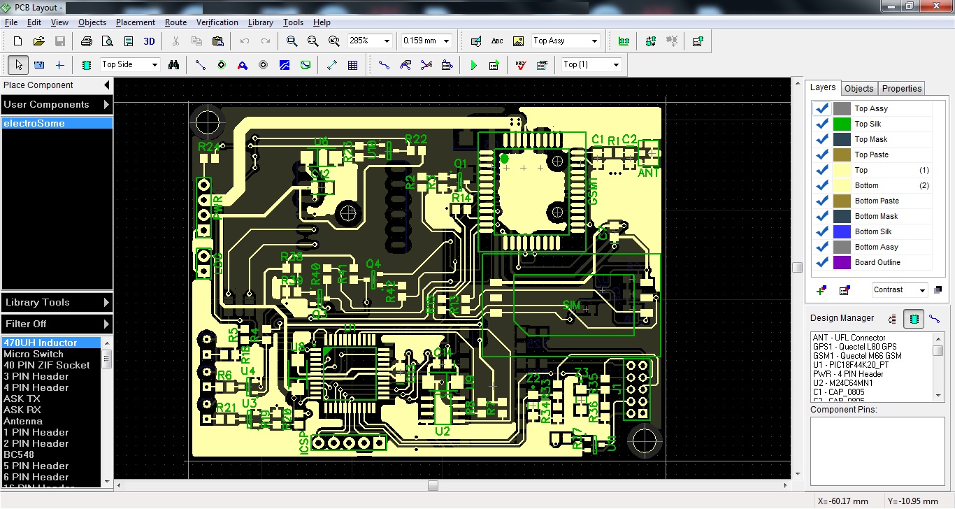
On the other hand, a PCB layout is a term designated to creating a whole virtual circuit board with accurate measurements and angles of the signal tracks, pad width, diameter of the holes, and component size and shape. A PCB layout represents and indicates the precise location of the components and the net of signal routes. In the PCB layout, we can see each signal track connecting two different points. The information about the layers management, ground, and power planes can be easily retrieved from the PCB layout because it stores all this information.
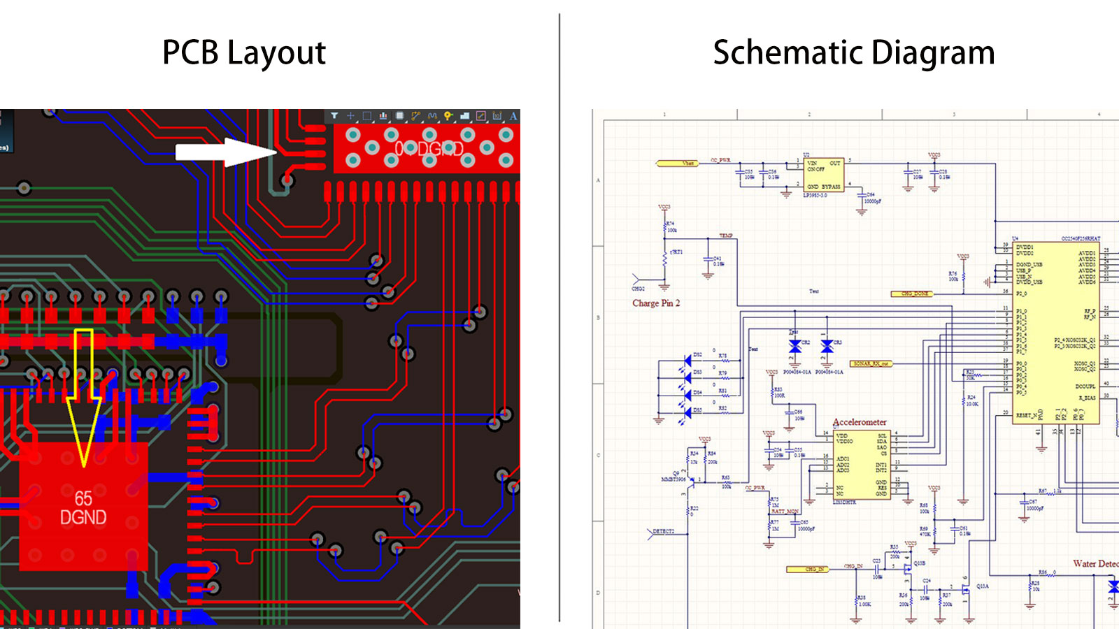
A substantial difference between the PCB schematic and layout is that a schematic is the first diagram drawn in the process of PCB designing. It contains 2-dimensional lines that arrange all the components connecting in an organized manner. On the other hand, a PCB layout is like a virtual circuit board that is okay to consider as a digital copy of the circuit. The layout is generated through a schematic. Without a schematic, it is almost impossible to design the layout as we will not have a defined pattern for component placement and developing signal tracks.
> Recommend reading: What is IPC Standard to PCB Layout Design?
The difference between the PCB schematic and layout is very fundamental. A PCB is usually a combination of multiple individual circuits that combines and forms a complex circuit board. The formation of a PCB design starts with the circuit diagrams, which is a raw form of a PCB schematic. The PCB layout also carries the same importance as representing all the essential information regarding the signal tracks, ground and power planes, component sizes, and their placements. Also, about the signal and power integrity of the circuit board.
A PCB schematic is quite easy to understand and clears the structure of the circuit board design. But, still, there are some key points to keep in mind about the schematic.
We have developed a clear understanding of the PCB schematic and layout. PCB schematic is the first stage of the production of a printed circuit board and contains all the connections of the circuit board in an organized one-by-one manner. However, we know that the PCB schematic and the printed circuit board look completely different. So, in this part of the article, we discussed the design aspects of the circuit board.
A PCB refers to a hard electronic circuit board with SMT or THT components assembled on it. The schematic may use to produce two types of PCBs rigid and flexible. The rigid PCBs are hardcore and non-foldable, whereas flexible PCBs are like a thin plastic film that can be folded easily to adjust into a congested place. Both rigid and flexible PCBs follow the same schematic but different layout design techniques.
The differences that are made in PCB layout by neglecting the schematic design include:
The PCB layout plays a significant role in defining the signal integrity and the behavior of current in a circuit. Minor changes in the layout of the PCB may change the output drastically. However, the major player that determines the signal integrity in a circuit board is frequency. The other factors include layer stack, planes, and vias management.
There is a fundamental rule, if even a small amount of current is released, it will always return to its source. Hence, the designers provide current return paths in the layout. If they do not do so, the current does not care. It will still return to its source, but at some cost. The unattended return current will interfere with the rest of the signals while finding its way back to its source.
These days to main signal integrity, the PCBs are routed over the ground plane to isolate signal layers from each other. It is also common to see that the return current is induced directly below a signal track, which is possible due to the substrate's parasitic capacitance. But we know that the capacitive impedance of a circuit is inversely proportional to a signal's frequency. Hence, when routed above a ground plane, the lower frequency signals induce less current directly below a signal trace.
In PCBs with a layout/stack that facilitates separate layers for signal, ground, and power planes, some of the return currents appear below the traces while the remaining current spread throughout the circuit board. After assembling all the components, it becomes more difficult to locate the current return path due to coupling issues. But we know, for low frequency, the grounded current selects the path of least resistance and for high frequency, the grounded current follows the least inductance route, which is located directly underneath the signal track because it has the smallest loop area.
We know that the current return path in a circuit depends on the frequency and the loop inductance depends on the path traveled by a signal as it returns to the ground, the loop inductance for a specific track also relays on frequency. However, in transmission line models, this concept is usually neglected as the general idea is that due to the high-frequency signal will follow the transmission line path. But, this concept leads to two issues.
The performance and outcome of a circuit depend equally on its schematic and layout. Even with an accurately designed schematic, it is possible not to have an ideal output. It happens due to these reasons:
External noise, signal integrity, and power dissipation are also some important aspects of a circuit to consider while heading to have an ideal output.
In short, even with a perfect schematic, you can still have a malfunctioning circuit board due to poor layout and stack-up management.
NextPCB has been offering a one-stop solution for PCB manufacturing, assembling, and testing services for over 15 years. We at NextPCB use the latest technology with every possible approach to carry out complex to waterproof high-level Interface Circuit Boards and offer a wide range of PCBs, including metal-core, LED, High-frequency, High-Speed, Waterproof PCBs, and PCB Cameras.
We at NextPCB offer a standard and waterproof PCB of up to 20 layers with the desired thickness and are willing to incorporate all unique requirements.
Geographically we are located in China. But in a decade and a half, we have built a trustworthy relationship with our worldwide clients.
Get in touch with us to learn about our PCB capabilities and to get an instant PCB quote.
Luckily the NextPCB provides a $0 Free 1-4 layer PCB Prototype service.
A PCB schematic is the first and the most essential document that contains information about each signal track and the components a signal path connects. A schematic is a 2-dimensional document and may consist of different pages. It describes from where a signal path start, connects with which other components and where it ends.
There is a fundamental difference between a schematic and a PCB layout. A PCB layout is like a 3D model of a circuit board, which contains accurate information about the component placement, their sizes, pads, signal tracks width, hole diameter, etc.
A PCB schematic is a blueprint for the layout. It is essential for reverse engineering the printed circuit board.

Still, need help? Contact Us: support@nextpcb.com
Need a PCB or PCBA quote? Quote now

