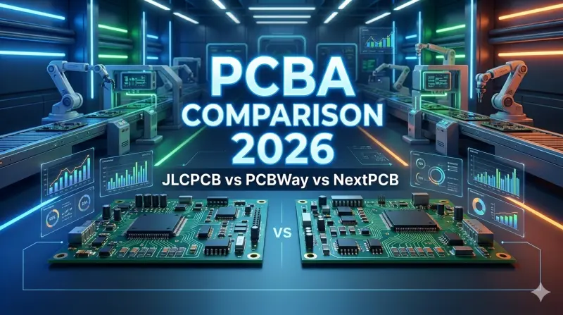
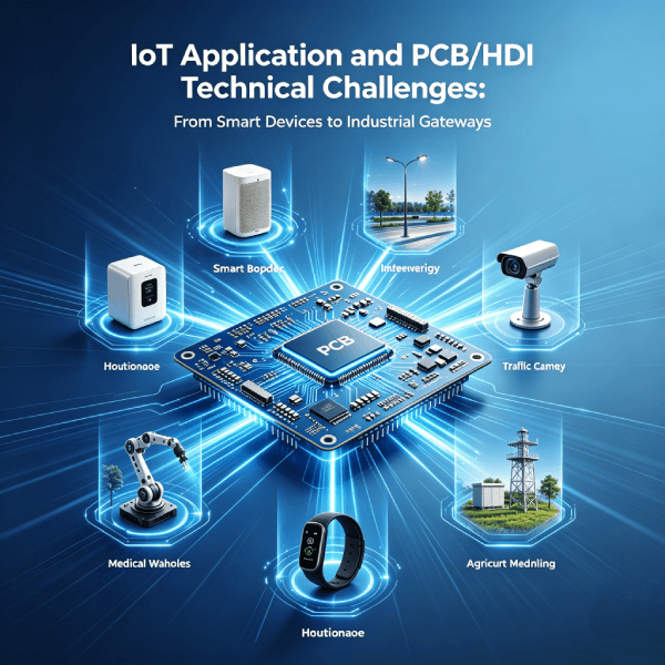
IoT Application and PCB/HDI Technical Challenges: From Smart Devices to Industrial Gateways
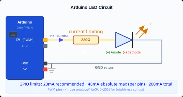
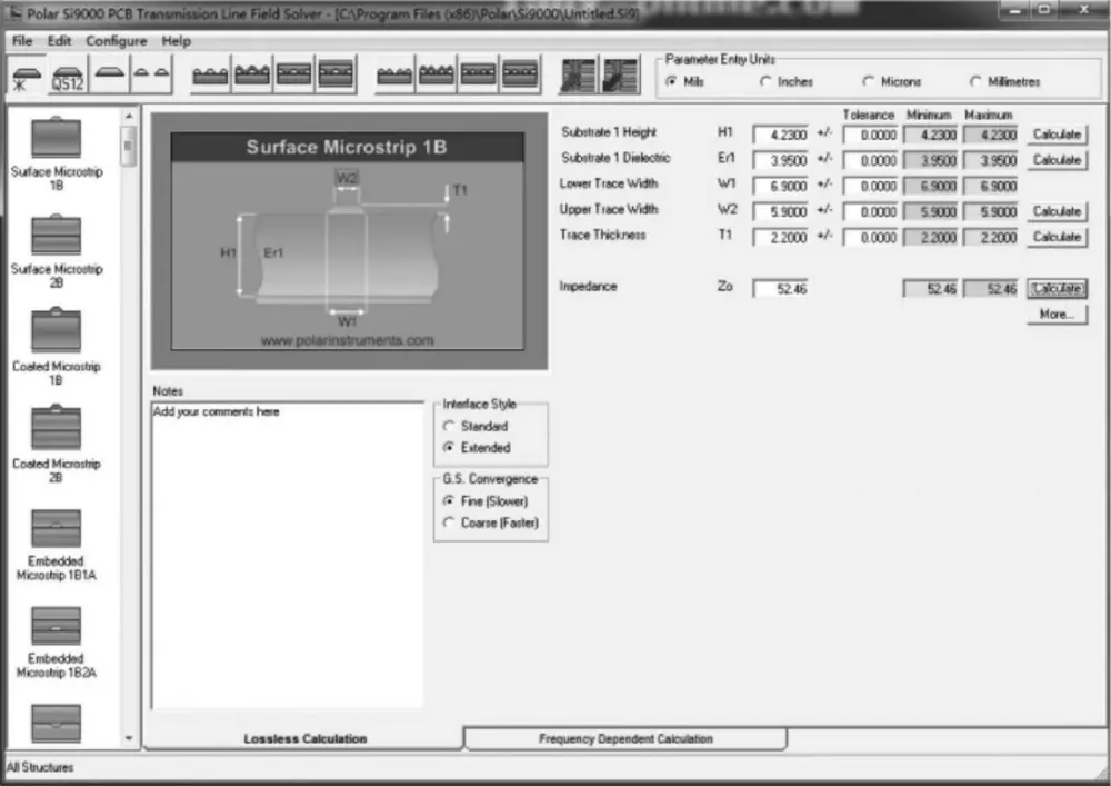
IoT is widely used in multiple fields such as home, city, industry, medical, and agriculture. By integrating devices and sensors through networks, IoT enables seamless data collection, transmission, and analytical decision-making. However, the true value of these applications depends on the reliable delivery of hardware in real-world environments. Modern HDI PCB technology, micro-via routing, impedance control, and manufacturing precision provide the essential foundation for high performance and high yield, making smart living and industrial automation a reality.


 NextPCB Capabilities
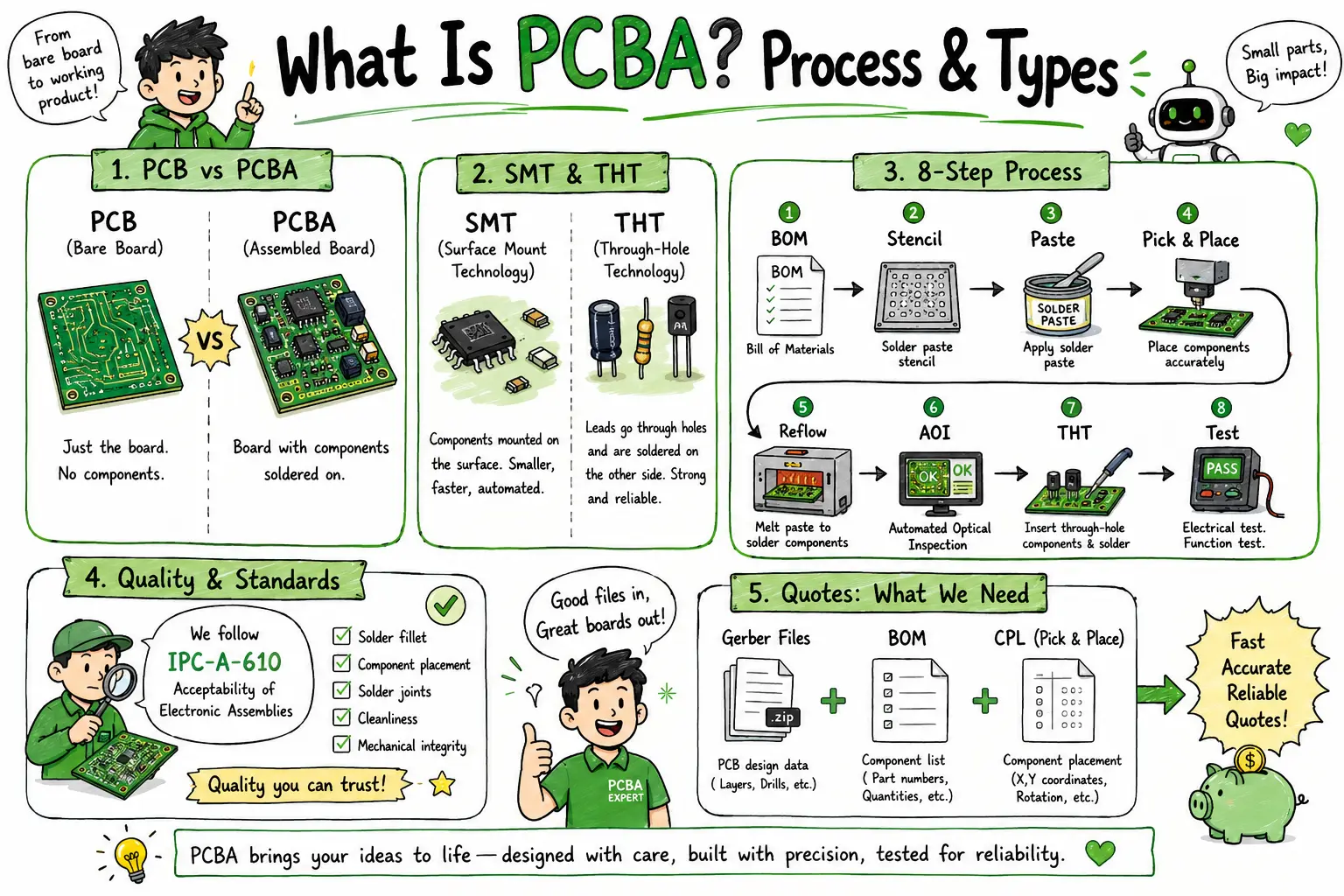
 PCB Assembly
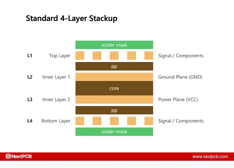
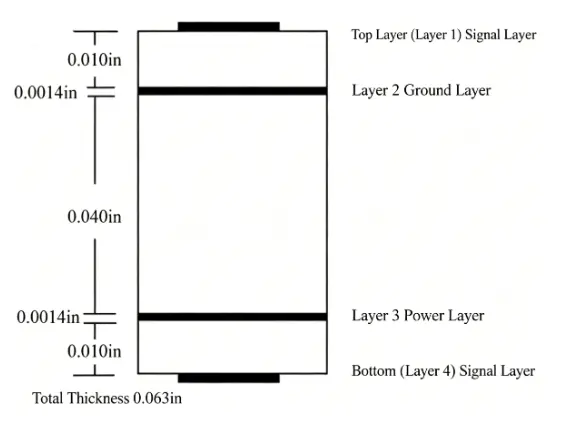
 Layer Buildup
 SMD-Stencils
 PCB Design-Aid & Layout
 Mechanics
 Surface
 Quality
 Drills & Throughplating
 Factory & Certificate