
 NextPCB Capabilities
Printed Circuit Boards
NextPCB Capabilities
Printed Circuit Boards
 PCB Assembly
 Layer Buildup
 SMD-Stencils
 PCB Design-Aid & Layout
 Mechanics
 Quality
 Drills & Throughplating
 Factory & Certificate
 PCB Assembly Factory Show
Certificate
PCB Assembly Factory Show
Certificate
Support Team
Feedback:
support@nextpcb.com


To successfully order PCB assembly (PCBA), you need to prepare four types of files: Gerber files, a BOM (Bill of Materials), a pick-and-place (CPL) file, and — for multilayer boards — a stackup specification. Get all four right, and the process is straightforward. Miss one, or send a file in the wrong format, and you're looking at delays, back-and-forth emails, and quotes that don't reflect your actual design.
You've finished your PCB layout. DRC passes clean. The schematic looks right. This is usually where things get less straightforward — because getting files from your design tool into a format a factory can actually use involves more steps than most tutorials cover.
In practice, you only need a small set of files — but each one has to be correct. This guide walks through what each file is, how to export it from KiCad, Altium, and EasyEDA, and what errors to catch before you submit.
For a standard turnkey PCB assembly order, you need four core file types:
| File | Purpose | Required For |
|---|---|---|
| Gerber + Drill files | Defines the bare board — copper, silkscreen, solder mask, outline | Fabrication |
| BOM (Bill of Materials) | Lists every component: part number, value, reference designator, footprint | Component sourcing + assembly |
| Pick-and-Place file (CPL) | X/Y coordinates, rotation, and layer for each SMT component | SMT machine programming |
| Stackup specification | Layer order, dielectric thickness, copper weight, impedance requirements | 4-layer+ boards or any impedance-controlled design |
Some manufacturers also request:
If you're ordering partial assembly (providing your own components), you'll also need to coordinate component packaging and labeling with the manufacturer separately.
Most engineers think of the stackup as a purely electrical concern — layer order, impedance, signal return paths. But your stackup has direct consequences for the assembly process too, and specifying it correctly upfront prevents problems at the factory.
Standard PCB thickness is 1.6mm. Most SMT assembly lines are calibrated for this. If your design uses a non-standard thickness — 0.8mm, 1.0mm, or 2.0mm — you need to call this out explicitly. Thin boards can flex or warp on conveyor systems, causing misalignment during pick-and-place. Thick boards may require fixture adjustments.
The copper weight in your stackup (typically 1oz for outer layers) influences how heat distributes across the board during reflow soldering. Heavy copper (2oz+) acts as a heat sink — especially on large copper pours or power planes — and may require an adjusted reflow profile to ensure all pads reach the correct peak temperature for reliable soldering. If you're using heavy copper for a power design, note this in your stackup specification.
Your surface finish choice — part of the stackup specification — directly affects solderability:
For most Arduino-style or IoT prototype boards, HASL works fine. If your design includes any ICs with pitch below 0.65mm, use ENIG.
For 4-layer and above, provide a simple stackup table:
| Layer | Name | Type | Copper Weight | Thickness |
|---|---|---|---|---|
| 1 | F.Cu | Signal | 1 oz | — |
| — | Prepreg | Dielectric | — | 0.1mm |
| 2 | In1.Cu | GND | 0.5 oz | — |
| — | Core | Dielectric | — | 1.2mm |
| 3 | In2.Cu | PWR | 0.5 oz | — |
| — | Prepreg | Dielectric | — | 0.1mm |
| 4 | B.Cu | Signal | 1 oz | — |
If you have impedance requirements, add a line specifying: target impedance (e.g., 50Ω single-ended), reference layer, trace width, and which net or signal group it applies to.
For standard 2-layer boards with no impedance requirements, a separate stackup document isn't necessary — the manufacturer's default stackup will apply.
If something goes wrong in a PCBA order, chances are it's in the BOM. Wrong part numbers, missing values, reference designators that don't match the layout — these are the issues that add days to a turnaround or cause a board to come back assembled with the wrong components. In real projects, most delays aren't caused by PCB fabrication. They come from BOM issues. For a deeper look at BOM structure and common formatting mistakes, see: What Is a BOM in PCB Design? How to Write One for PCBA.
If you need a practical walkthrough focused on preparing a production-ready BOM from scratch, including file organization and handoff requirements, see: How to Prepare PCB Files for Assembly: Gerber, BOM, Stackup & More
Group identical components on a single row. Each row should have:
Optional but helpful:
>> BOM Sample: If you need to order PCB assembly order in NextPCB, please give us the BOM list as BOM Sample. Download ↓
Recent versions of KiCad introduced an improved BOM exporter with better field management. In KiCad 10:
Best practice: Add an “MPN” custom field to every symbol in your schematic before starting layout. Filling in part numbers during schematic capture takes 2 minutes per component; hunting them down before an order takes 30 minutes or more.
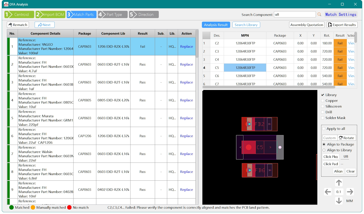
NextPCB HQDFM DFA analysis pick and place centroid file editing
A pick-and-place file (also called a CPL file — Component Placement List — or centroid file) is a text file that tells the SMT assembly machine exactly where to place each component on the board. For step-by-step export instructions across all major tools, see: Pick-and-Place File Guide: KiCad / Altium / EasyEDA Export and How to Create a Centroid File Instantly.
Each row contains:
Without this file, the assembly house has to manually measure component positions from your Gerbers — a slow, error-prone process that most manufacturers charge extra for (or simply refuse to do for complex boards).
>> Pick & Place File Sample: please send us to pick and place file when the order assembly project to us. Download ↓
KiCad 10 note: The updated placement exporter now includes a “merge top and bottom” option that outputs a single file with a Layer column. This is cleaner for manufacturers who prefer a consolidated CPL.
These are the most frequent issues assembly houses flag when reviewing submitted packages — and most are preventable.
The single most common delay. If your BOM says “100nF capacitor, 0402” without a manufacturer part number, the assembler either has to ask you or substitute a part that may have different electrical characteristics. Always include full MPNs.
If your BOM lists C1 but your PCB has no C1 (renamed to C101 during layout), the assembler can't match components to positions. Keep reference designators synchronized between schematic, BOM, and PCB at all times.
A Gerber package without an Edge.Cuts (board outline) file forces the manufacturer to estimate the board boundary, which can result in incorrect panelization or routing. Always include the Edge.Cuts layer.
If your PCB origin in the design tool doesn't match the manufacturer's expected reference point, all component coordinates will be offset. Use the bottom-left corner of the board outline as the origin, or confirm the expected reference with your manufacturer.
If your BOM includes components but the Gerber solder mask layer doesn't have openings for those pads, components can't be soldered reliably. This usually happens when footprints are copied from unofficial libraries. Always verify solder mask apertures in your Gerber viewer before submitting.
If your design has variants (some components populated, some not), make sure your CPL file only includes components that should actually be assembled. An assembler placing a DNP component is harder to fix than a missing one.
Some first-time buyers upload .kicad_pcb or .pcbdoc files directly. While some manufacturers can convert these, many cannot — and the conversion may not be exact. Always export Gerbers explicitly.
Understanding this distinction helps you scope your order correctly.
The manufacturer handles everything:
You provide: Gerber files, BOM with MPNs, CPL file, stackup spec.
Best for: Designs where you don't want to source components yourself, production-intent prototypes, or any run where assembly quality and traceability matter.
Cost structure: You pay for bare board + component cost (with a markup) + assembly labor. Component markups at assembly houses are typically 10–30% above distributor cost.
You supply the components; the manufacturer assembles them.
You provide: All of the above, plus physically packaged and labeled components (typically in tape-and-reel or cut tape).
Best for: Situations where you have specific component sources or have already purchased parts. Also useful when some components are difficult to source through standard channels (custom inductors, specific RF modules, etc.).
Cost structure: Assembly labor + bare board only. No component markup, but you absorb inventory risk and logistics overhead.
For most first-time PCBA orders, turnkey is simpler — you don't have to manage component procurement, and the manufacturer assumes responsibility for sourcing accuracy. For higher-volume production where component cost matters, partial assembly may be worth the added logistics.
Once your file package is ready, getting a quote takes a few minutes:
If the online system can't match a component in your BOM (discontinued part, regional availability issue), a sales engineer will contact you with an alternative before production starts. This review happens before any manufacturing begins, not after.
PCB fabrication (or PCB manufacturing) produces the bare board — the physical substrate with copper traces, solder mask, and silkscreen, but no components. PCB assembly (PCBA) takes that bare board and solders all the electronic components onto it. You can order fabrication-only (for boards you'll assemble yourself) or turnkey PCBA (fabrication + assembly from one supplier).
For standard 2-layer boards without impedance requirements, no — the manufacturer applies their default stackup. For any 4-layer+ design, or any board with controlled impedance traces (USB, HDMI, RF, DDR), you must provide a stackup document specifying layer order, dielectric thickness, copper weight, and impedance targets. Omitting this causes the manufacturer to fabricate with a generic stackup that may not meet your signal integrity requirements.
CSV or Excel (.xlsx) are the most universally accepted formats. The file must have clearly labeled columns — Reference Designator, Quantity, Value, Package/Footprint, and Manufacturer Part Number (MPN) at minimum. Avoid merged cells or color-coded formatting in Excel; plain tabular data is easiest for assembly systems to parse.
A pick-and-place file (CPL) lists the X/Y coordinates, rotation angle, and layer (top/bottom) of every SMT component on your board. Assembly machines use this to program their component placement heads. Every major PCB design tool can export it: in KiCad 10 go to File → Fabrication Outputs → Component Placement; in Altium go to File → Assembly Outputs → Pick and Place Files; in EasyEDA go to Fabrication → Pick and Place File.
For a typical IoT or microcontroller board — 2-layer, around 100 × 100mm, 30–50 SMT components, 10 pieces — expect roughly $150–$350 total, including bare board, components, and assembly labor. That range shifts considerably based on IC complexity: a board with fine-pitch QFPs or BGA packages costs more due to additional fixture and handling requirements. Double-sided SMT adds another step and associated cost. For a full cost breakdown with 2026 pricing, see: How Much Does PCB Assembly Cost? (2026 Price Guide). Use an online PCBA quote tool with your actual BOM for a meaningful number — the spread across different designs is too wide for generic estimates to be useful.
Turnkey PCBA means the manufacturer sources all components and handles fabrication and assembly end-to-end. Partial assembly (or consigned assembly) means you supply the components and the manufacturer handles only fabrication and soldering. Turnkey is simpler for prototypes; partial assembly gives you more component control and can reduce cost at higher volumes.
Some manufacturers accept KiCad native files, but it's not reliable across all vendors. Always export proper Gerber files, a BOM in CSV/Excel format, and a CPL file from KiCad's fabrication output tools. This ensures compatibility with any manufacturer's workflow and prevents conversion errors. KiCad 10 makes this export process straightforward — the whole package can be generated in under 10 minutes.
Preparing a PCBA file package isn't complicated, but the details matter. The four core files — Gerbers, BOM with MPNs, CPL, and stackup spec for multilayer boards — give a manufacturer everything they need to build your board without guessing.
The most time you'll spend on this is the first time. Once you've done it once, subsequent orders follow the same steps and take a fraction of the effort.
If your files are ready, or you want to check pricing before finalizing your design:
Upload Files & Get a Free PCBA Quote →
Turnkey and partial assembly supported. Free DFM review included.
>> Recommend reading: How to generate pick and place (centroid) files in KiCad? (Updated for KiCad 9)
Still, need help? Contact Us: support@nextpcb.com
Need a PCB or PCBA quote? Quote now


 Surface

