
 PCB Assembly
 Layer Buildup
 Online Tools
 PCB Design-Aid & Layout
 Mechanics
 SMD-Stencils
 Quality
 Drills & Throughplating
 Factory & Certificate
 PCB Assembly Factory Show
Certificate
PCB Assembly Factory Show
Certificate
Support Team
Feedback:
support@nextpcb.com


Most engineers treat the stackup as a signal integrity problem. Pick a layer count, set impedances, route the board, and move on. That logic works fine until your boards come back from assembly warped, or your fine-pitch ICs don't solder cleanly, or the factory emails you asking what stackup they should use — three days after you thought the order was confirmed.
The stackup specification connects your electrical design to the physical manufacturing process. It's not just a document for the PCB fab shop. It directly shapes what happens on the SMT line: how the board behaves in a reflow oven, whether the surface finish is compatible with your component pitches, and whether the board stays flat enough for pick-and-place to work reliably.
This guide covers what a stackup specification needs to include for SMT assembly, why each parameter matters, and what to get right before you send files.
A stackup specification is a document — usually a table or drawing — that defines the physical structure of your PCB layer by layer: the order of copper layers and dielectric layers, the thickness of each, the copper weight, the base material, and any controlled impedance requirements. It also typically includes surface finish selection and board thickness tolerance.
For 2-layer boards without impedance requirements, most manufacturers apply a default stackup, and you don't need to provide one. For any 4-layer or higher board, or any design with controlled impedance traces, you must specify the stackup explicitly. Without it, the manufacturer fabricates with whatever parameters meet your layer count and thickness — which may or may not match what your signal integrity calculations assumed.
The stackup also feeds directly into SMT process decisions:
None of these are purely electrical concerns. They're process constraints, and the stackup is where you communicate them.
For most digital and mixed-signal designs, a 4-layer board with a 1.6mm total thickness is the default choice. The standard layer assignment looks like this:
| Layer | Name | Function | Copper Weight |
|---|---|---|---|
| 1 | F.Cu (Top) | Signal / Components | 1 oz |
| — | Prepreg | Dielectric | — |
| 2 | In1.Cu | GND plane | 0.5 oz |
| — | Core | Dielectric | — |
| 3 | In2.Cu | PWR plane | 0.5 oz |
| — | Prepreg | Dielectric | — |
| 4 | B.Cu (Bottom) | Signal / Components | 1 oz |
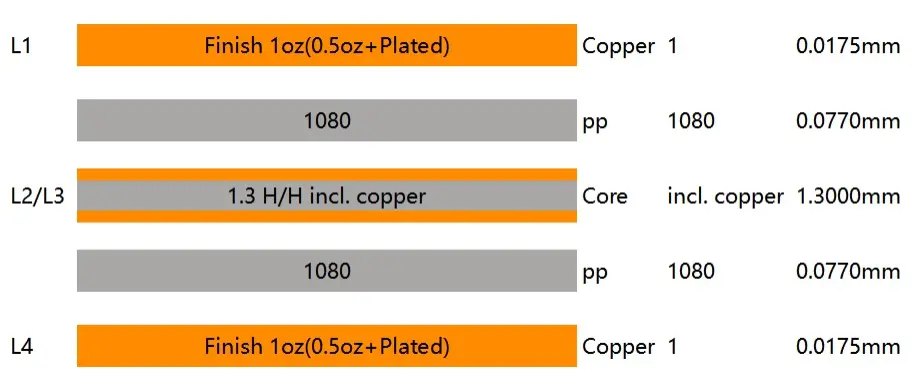
NextPCB 1.6mm 4-Layer Standard Stackup Diagram
Why this arrangement? Layer 2 as GND provides a continuous return path directly beneath the top signal layer — critical for controlling trace impedance and minimizing loop inductance. Layer 3 as PWR sits adjacent to GND, forming a distributed capacitance that helps with power delivery network (PDN) performance. Both inner planes are at 0.5 oz because they're not carrying high current; keeping them thinner allows more room in the dielectric budget for controlled-impedance prepreg thickness.
For power designs or boards carrying more than 2A on inner planes, inner layer copper should move to 1 oz. Note this in your stackup specification.
Typical Thickness Breakdown (1.6mm total)
| Layer | Thickness |
|---|---|
| F.Cu (copper) | 35 µm (1 oz) |
| Prepreg | 0.10 mm |
| In1.Cu (copper) | 17.5 µm (0.5 oz) |
| Core | 1.265 mm |
| In2.Cu (copper) | 17.5 µm (0.5 oz) |
| Prepreg | 0.10 mm |
| B.Cu (copper) | 35 µm (1 oz) |
| Total | ~1.6 mm |
This is the stackup most manufacturers apply by default for 4-layer FR-4 boards at 1.6mm. If you don't specify, this is probably what you get — which is fine for most designs. The problems start when your design assumes a different prepreg thickness for impedance reasons, or you need a thinner core for controlled coupling between layers, and you never put it in writing.
Thickness stops being a purely mechanical parameter once you're on an SMT line. At 0.8mm, boards start to flex on standard conveyor rails — enough to cause pick-and-place misalignment and stress solder joints during cooling. At 2.4mm and above, they stop fitting standard magazine stacking for automated loading, and the extra thermal mass changes what the reflow profile needs to look like. Neither deviation shows up in your schematic, but both show up immediately in production. If your design requires a non-standard thickness, call it out in your stackup spec — not as a footnote in a purchase order.
Heavy copper behaves like a heat sink during reflow — it pulls heat away from pads and into large copper areas. On 2 oz outer layers, you'll often see pads lag behind the reflow profile: the oven temperature is climbing, but the pad hasn't reached liquidus yet because the surrounding copper is soaking up the heat. The result is cold joints that look fine visually but fail in thermal cycling. If you're running 2 oz outer copper on a power design, document it in the stackup spec and flag it to your assembly house. Most can tune the profile for it — but only if they know to look for it.
IPC-6012 allows up to 0.75% bow and twist for most SMT assemblies. In practice, many assemblers tighten this to 0.5% for BGA-heavy designs — and it's usually where they push back first if your stackup is asymmetric. Out-of-plane warpage causes BGA balls to lose contact with pads before reflow is complete, which is exactly the kind of failure that doesn't show up in visual inspection.
The primary cause of bow and twist is asymmetric stackup — copper layers that are not mirrored about the board's mid-plane. An unbalanced copper distribution creates unequal stress during the lamination and reflow thermal cycles, and the board warps.
Rules for maintaining stackup symmetry:
In your stackup specification, include an explicit note confirming that the stack is symmetric, or flag any asymmetric layers and explain why they're necessary.
FR-4 laminate comes in standard Tg (~135–140°C) and high-Tg (≥170°C) grades. For lead-free reflow (SAC305, peak temperature around 245–260°C), standard Tg FR-4 can handle the process — the Tg isn't the melting point, and FR-4 is stable well above its Tg at reflow timescales.
What Tg actually governs is how many reflow passes the board can tolerate before the laminate starts to degrade:
Specify the required Tg in your stackup document. Most manufacturers default to standard Tg unless you ask otherwise. High-Tg adds a small cost premium — typically 5–15% on material cost.
Surface finish is defined as part of the stackup specification, and it has a direct impact on solderability, component compatibility, and shelf life before assembly.
| Finish | Solderability | Flatness | Shelf Life | Best For |
|---|---|---|---|---|
| HASL (Pb-free) | Good | Poor | 12 months | General through-hole, large-pitch SMT |
| ENIG | Excellent | Excellent | 12 months | Fine-pitch SMD, BGA, QFN |
| OSP | Good | Excellent | 6 months | High-volume production, cost-sensitive |
| ENEPIG | Excellent | Excellent | 12 months | Wire bonding + SMT mixed assembly |
| Immersion Silver | Good | Excellent | 6 months | RF boards, high-frequency design |
HASL deposits solder unevenly across pads — the surface profile has peaks and valleys that become a reliability risk at pitches below 0.65mm. On 0.5mm pitch QFP or QFN, HASL pad coplanarity variance can prevent the stencil from seating correctly during paste printing, leading to bridging or insufficient paste. For prototypes with only 0603 passives and SOT-23 discretes, HASL is fine and saves money. For anything with fine-pitch ICs, use ENIG.
ENIG provides a flat, oxidation-resistant surface ideal for SMT. The nickel barrier layer prevents gold diffusion into the solder joint, and the gold layer provides excellent initial wettability. One failure mode to be aware of: black pad syndrome — a phosphorus-enriched nickel layer that forms under the gold during plating and causes brittle, non-wetting joints. If you're working on high-reliability designs, it's worth asking your supplier about their ENIG process control or past black pad incidents. Most reputable manufacturers have this dialed in, but it's the kind of thing you verify once and then stop worrying about.
>> Recommend reading: HASL vs ENIG: An Ultimate Guide on Surface Finish
OSP is the right choice for high-volume production where boards are assembled quickly after delivery. The organic coating burns off cleanly during reflow, leaving bare copper that wets well. The shelf life constraint (typically 6 months, sometimes as short as 3 months after opening) means OSP is risky for prototype boards that may sit on a shelf for months before assembly.
For most prototype and low-volume PCBA orders, ENIG is the default recommendation. It handles the widest range of component types, stores well, and the cost premium over HASL on small quantities is minimal.
Impedance control means the manufacturer measures trace impedance on test coupons and adjusts dielectric thickness or copper etching to hit your target. Not every design needs it, but these signal types always do:
If your design includes any of these, your stackup specification must include:
A stackup specification without these details forces the manufacturer to guess your intent, or to fabricate without impedance control and simply hope the default works.
The stackup specification doesn't have to be a formal document. In practice, most manufacturers accept:
At minimum, your stackup document should include:
| Parameter | What to Specify |
|---|---|
| Total board thickness | e.g., 1.6mm ±10% |
| Layer count | e.g., 4-layer |
| Layer sequence | Layer name, type (signal/plane), copper weight per layer |
| Dielectric thickness | Prepreg and core thickness per layer |
| Base laminate | e.g., FR-4 standard Tg, FR-4 high-Tg (170°C+), Rogers 4003C |
| Surface finish | HASL, ENIG, OSP, etc. |
| Controlled impedance | Target value, reference layer, tolerance, affected nets |
| Tg requirement | If above standard |
| Bow and twist limit | If tighter than IPC default 0.75% |
For 2-layer boards without impedance requirements, a note in your order saying "standard stackup, 1.6mm, 1 oz outer copper, ENIG finish" is sufficient. The manufacturer's default handles the rest.
Q: Do I need a stackup specification for a 2-layer board?
For a standard 2-layer board with no impedance requirements, no. The manufacturer will apply their default stackup (1.6mm total, 1 oz outer copper, standard FR-4). If you have specific thickness requirements, controlled impedance (e.g., an RF trace or USB differential pair), or non-standard copper weight, you should document it.
Q: What's the difference between prepreg and core in a PCB stackup?
Core is a rigid, fully cured fiberglass-reinforced epoxy sheet with copper foil on both sides. Prepreg (pre-impregnated) is a fiberglass sheet with partially cured epoxy — it's the adhesive layer that bonds cores together during lamination. In a 4-layer board, the two inner copper layers are etched onto a core; the outer layers are bonded to the core via prepreg during the lamination press.
Q: How do I know if my design needs controlled impedance?
Check whether you're routing any high-speed serial protocols (USB, HDMI, PCIe, DDR), RF or antenna traces, or any differential pairs operating above ~100MHz. If yes, those traces need controlled impedance. If your design is purely through-hole or low-speed (I2C, SPI at standard voltages, UART), controlled impedance is typically not required.
Q: What is PCB bow and twist, and why does it matter for SMT?
Bow and twist are measures of out-of-plane deformation in a PCB. Bow is a curvature across the board; twist is a rotation about the diagonal. During SMT assembly, a warped board doesn't sit flat on the conveyor or fixture — this causes pick-and-place misalignment, paste printing inconsistency, and incomplete BGA solder ball contact during reflow. IPC-6012 specifies a maximum of 0.75% for SMT assemblies. BGA-heavy boards often require 0.5% or tighter.
Q: Can I use Rogers or other high-frequency laminates in a standard SMT assembly process?
Yes, but with caveats. Rogers materials (4003C, 4350B, etc.) have different Tg values, CTE characteristics, and drill behavior than FR-4. They're compatible with standard lead-free reflow, but the assembly house needs to know the material so they can adjust their drill speeds, depaneling method, and reflow profile if needed. Always disclose non-FR-4 laminates in your stackup specification.
Getting the stackup specification right is one of the most leveraged things you can do before sending files for assembly. It's not a long document — for most 4-layer boards, a single table covers everything the manufacturer needs. But the information in that table — copper weight, dielectric thickness, surface finish, impedance targets — determines whether your boards come back flat, solderable, and electrically correct.
The engineers who have the most consistent results aren't necessarily the ones who spend the most time on layout. They're the ones who communicate clearly with the factory about what the board needs to be.
If you're working on a multilayer or impedance-controlled design, it's usually worth getting the stackup reviewed before fabrication — especially if the board will go through multiple reflow cycles or uses fine-pitch components. Most assembly houses can review the stackup alongside your Gerbers and flag potential issues early. If you want a second set of eyes on it, send it over.
Still, need help? Contact Us: support@nextpcb.com
Need a PCB or PCBA quote? Quote now


 Printed Circuit Boards
 Surface

