
 NextPCB Capabilities
Printed Circuit Boards
NextPCB Capabilities
Printed Circuit Boards
 PCB Assembly
 Layer Buildup
 SMD-Stencils
 PCB Design-Aid & Layout
 Mechanics
 Quality
 Drills & Throughplating
 Factory & Certificate
 PCB Assembly Factory Show
Certificate
PCB Assembly Factory Show
Certificate
Support Team
Feedback:
support@nextpcb.com


The Arduino Nano remains a cornerstone for hardware prototyping, celebrated for its compact form factor and robust capabilities. However, transitioning a prototype from a breadboard to a reliable, mass-produced printed circuit board (PCB) requires a deep understanding of the Arduino Nano pinout diagram and underlying electrical constraints.
While many tutorials focus on basic hobbyist setups, this guide is engineered for hardware developers. Whether you are designing a custom carrier board, an industrial IoT gateway, or integrating the bare ATmega328P microcontroller into a proprietary PCBA, relying solely on basic wiring is insufficient. This guide explores the complete pinout functionality and bridges the gap between prototyping and commercial manufacturing, highlighting critical Signal Integrity (SI), Electromagnetic Compatibility (EMC), and Design for Manufacturability (DFM) principles.
>> Recommend reading: Arduino Nano Technical Specifications

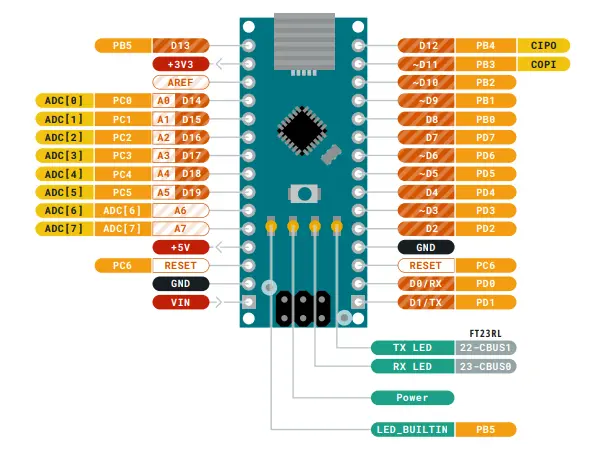
Standard top-down view of the Arduino Nano highlighting the primary digital and analog pin assignments for physical assembly.
Before diving into pin-level routing, it is crucial to select the right processing core for your application's architecture.
Engineering Tip: From a PCB layout perspective, both share a nearly identical footprint, but pin multiplexing and internal architecture differ, which may impact compatibility in certain designs. Furthermore, if you directly integrate the microcontroller, the ATmega4809 requires different decoupling capacitor placements and clock routing schemes compared to the ATmega328P.
Standard top-down view of the Arduino Nano highlighting the primary digital and analog pin assignments.
Source: Arduino Official Pinout Documentation
Understanding the pinout is just the first step. Knowing how to route these signals on a custom PCB determines the reliability of your final product.
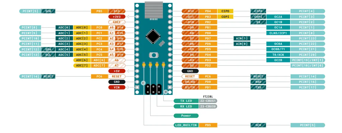
Comprehensive pinout diagram including secondary functions such as Interrupts (PCINT) and Analog-to-Digital Converter (ADC) channels.
Source: Arduino Official Pinout Documentation
The Nano features 14 digital I/O pins capable of handling general logic. Six of these (D3, D5, D6, D9, D10, D11) support hardware Pulse Width Modulation (PWM).
These 8 pins connect to the internal 10-bit Analog-to-Digital Converter (ADC), reading variable voltage levels (typically 0–VREF, often 5V or 3.3V depending on system configuration).
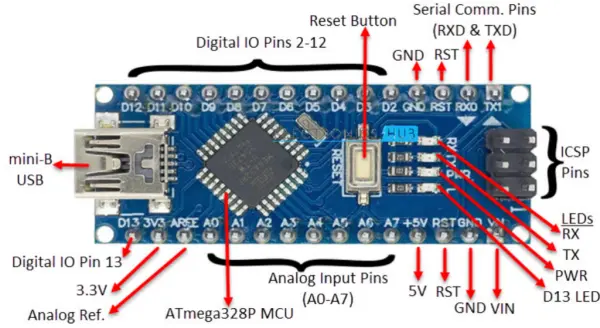
Comprehensive pinout diagram including mapping for the ATmega328P microcontroller, reset logic, and onboard indicator LEDs.
Proper power management dictates system stability. The Nano provides VIN (7-12V input), 5V (regulated output/input), and 3.3V (typically derived from the USB interface chip or onboard regulator, depending on the Nano variant).
Reliable data transfer is critical for IoT and consumer electronics.

Detailed mapping of communication protocols (SPI, I2C, and UART), critical for planning signal routing and data bus topology on custom PCB designs.
Building a prototype with jumper wires is easy; designing a board that scales to 10,000 units with a high yield requires strict adherence to Design for Manufacturability (DFM).
When moving to mass production, consider eliminating the physical Arduino Nano module entirely. Directly integrating the bare microcontroller (ATmega328P or ATmega4809) onto your custom PCBA eliminates mechanical failure points from header pins and allows for highly optimized layout. This can significantly reduce BOM cost (often by 30–50% per unit) and improve long-term reliability.
When partnering with an advanced manufacturer like NextPCB for your custom Arduino carrier boards or full standalone PCBA integration, structuring your layout to match standard manufacturing capabilities ensures lowest cost and highest reliability:
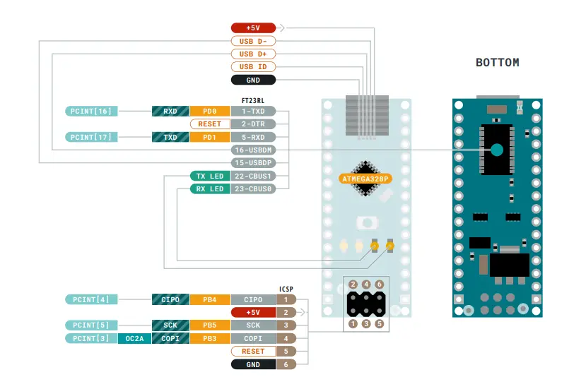
Bottom view of the Arduino Nano showing the ICSP header connections and the ATmega328P package orientation.
Source: Arduino Official Pinout Documentation
While mastering an 8-bit ATmega328P is foundational for hardware engineers, the trajectory of modern digital infrastructure rapidly scales beyond basic microcontrollers. As hardware designers progress into enterprise networking, AI hardware, and data center architectures, they encounter Application-Specific Integrated Circuits (ASICs). Unlike general-purpose microcontrollers, ASICs are custom-designed for highly specific systems, delivering superior performance, power efficiency, and size advantages. The physical integration of these high-end chips introduces extreme routing and manufacturing challenges.
High-end networking ASICs are the core engines pushing printed circuit board and substrate technologies toward the Ultra-High Density Interconnect (UHDI) standard. To support the massive I/O pin-outs and extreme signal densities of these advanced ASICs, the underlying PCBs and carrier substrates must possess extraordinary physical characteristics:
Every time a new generation of high-end ASIC is released, it forces PCB designers to solve massive layout puzzles: mapping an exponentially higher number of pin-outs, routing through more layers and microvias, all while dealing with shrinking available board space to accommodate internal logic complexities.
These UHDI-grade ASICs serve as the beating heart of modern digital infrastructure. Their high-speed computational and switching capabilities are essential for:
Interestingly, the push for extreme performance has sparked a technological return to fundamental principles. We are currently witnessing a revival in analog computing. The development and deployment of new Analog Computing ASICs (AC ASICs)—such as the highly publicized novel architectures pioneered by IBM—mark a true renaissance in this field. These analog chips process massive amounts of AI inference data highly efficiently at the physical level, requiring equally specialized and pristine PCB environments to preserve signal integrity without the discrete safety net of binary logic.
The staggering complexity of high-end networking ASICs is forcing a complete merger between traditional PCB manufacturing and semiconductor packaging technologies:
Can I use all Arduino Nano pins simultaneously?
No. Many pins have multiplexed functions. For example, if you use the SPI bus, pins D10-D13 are occupied. Furthermore, attempting to draw maximum current from all digital pins simultaneously will exceed the microcontroller's total package dissipation limit, leading to thermal failure.
What is the maximum power output of the 5V pin?
If powered via USB, it is limited by the USB port's capability. If powered via VIN, the onboard linear regulator limits the current. Depending on the input voltage (due to thermal dissipation), drawing more than 300mA–500mA continuously can cause the voltage regulator to overheat. Route heavy loads through separate, dedicated switching power supplies on your custom PCB.
Are analog pins strictly for analog inputs?
No. Pins A0 through A5 can also be defined in software and utilized as standard digital I/O pins if you run out of digital headers. However, A6 and A7 are purely analog inputs tied directly to the ADC multiplexer.
Mastering the Arduino Nano pinout diagram is the foundation of brilliant hardware design. However, the true leap in product development occurs when you apply professional PCB routing, signal integrity principles, and strict DFM checks to your designs.
Whether you are replacing an ATmega328P module on a 2-layer board to save BOM costs, or eventually scaling up to route complex high-speed ASICs on a multi-layer UHDI substrate, the underlying rules of physics remain the same. By designing your custom carrier boards and PCBAs with manufacturing in mind from day one—managing return paths, optimizing stackups, and controlling impedance for RF/USB lines—you mitigate prototyping risks, prevent costly respins, and accelerate your time to market. Partner with experienced manufacturers like NextPCB early in the design phase to leverage their advanced engineering support, turning your Arduino prototype into an industrial-grade product.
Still, need help? Contact Us: support@nextpcb.com
Need a PCB or PCBA quote? Quote now


 Surface

