
 NextPCB Capabilities
Printed Circuit Boards
NextPCB Capabilities
Printed Circuit Boards
 PCB Assembly
 Layer Buildup
 SMD-Stencils
 PCB Design-Aid & Layout
 Mechanics
 Quality
 Drills & Throughplating
 Factory & Certificate
 PCB Assembly Factory Show
Certificate
PCB Assembly Factory Show
Certificate
Support Team
Feedback:
support@nextpcb.com


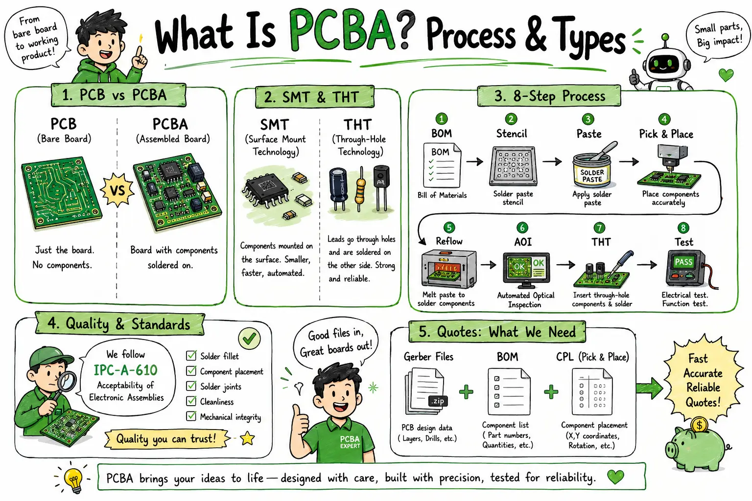
PCBA (Printed Circuit Board Assembly) is the process of soldering electronic components onto a bare PCB to create a working circuit board. It differs from a bare PCB in that all components — ICs, resistors, capacitors, connectors — are mounted and interconnected. The full process covers 8 steps: from BOM review and stencil printing through SMT placement, reflow soldering, AOI inspection, through-hole insertion, wave soldering, and functional testing. To get a PCBA quote, you need three files: Gerbers, a BOM, and a Pick-and-Place file.
These two terms are often used interchangeably, but they describe two completely different physical objects. Understanding the distinction is the first step before placing any assembly order. > Detailed Comparison here: PCB vs PCBA
A PCB (Printed Circuit Board) is the bare substrate — an engineered laminate (typically FR-4) with copper traces, vias, and pads etched or deposited to create electrical pathways. At this stage, the board performs no electrical function. It is essentially a road network with no vehicles on it.
A PCBA (Printed Circuit Board Assembly) is the same bare PCB after all electronic components have been soldered to it. This includes surface-mount devices (SMDs), through-hole components, connectors, and sometimes press-fit or mechanically attached parts. Once assembled, the board can receive power and execute its designed electrical function.
| Attribute | PCB (Bare Board) | PCBA (Assembled Board) |
|---|---|---|
| Definition | Bare substrate with copper traces | PCB with all components soldered on |
| Functional? | No | Yes (when powered) |
| Components | None | ICs, resistors, capacitors, connectors, etc. |
| Typical deliverable | Gerber files → fabrication | Gerbers + BOM + CPL → assembly |
| Cost driver | Layer count, board size, material | Component cost, placement complexity |
| Lead time (prototype) | 24 hrs – 5 days | 5 – 10 business days |
| IPC standard | IPC-6012 | IPC-A-610 |
Quick rule of thumb: If it has components on it, it's a PCBA. If it's blank copper and substrate, it's a PCB.
For engineers who already understand this distinction and want a deep operational guide covering DFM, DFA, and supplier selection, see our Ultimate PCB Assembly Guide →
Not all PCBA is created equal. The assembly method is determined by the component package types in your design. Getting this wrong at the quoting stage causes delays, cost overruns, and engineering holds.
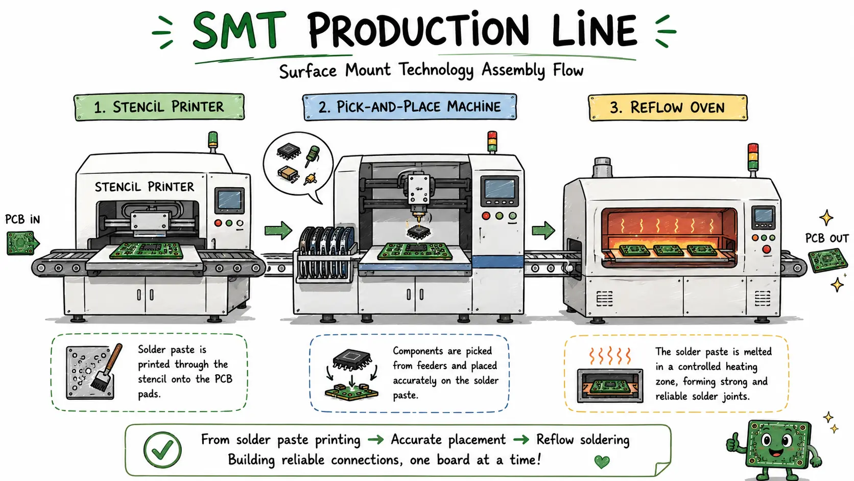
SMT is the dominant assembly method in modern electronics. Components — resistors, capacitors, ICs in QFP/BGA/LGA packages, MOSFETs — are mounted directly onto pads on the surface of the PCB.
How it works: Solder paste is printed through a stencil onto the pads. A pick-and-place machine positions each SMD component with sub-millimeter accuracy. The board then passes through a reflow oven where controlled heat profiles melt and solidify the paste, forming permanent solder joints.
Best for: Consumer electronics, IoT devices, compact designs, high-volume production, double-sided boards, fine-pitch ICs.
Key specs at NextPCB:
THT components have leads that pass through drilled holes in the PCB and are soldered on the opposite side. Common THT parts include electrolytic capacitors, connectors, power transistors, inductors, and legacy DIP ICs.
How it works: Components are inserted into plated through-holes either manually (for prototypes or low volume) or via automated insertion equipment. Soldering is performed using a wave soldering machine — the board is conveyed over a standing wave of molten solder that simultaneously wets all exposed leads — or by selective soldering for mixed boards.
Best for: High-current power components, mechanical stress applications (connectors, edge interfaces), harsh-environment boards, legacy designs.
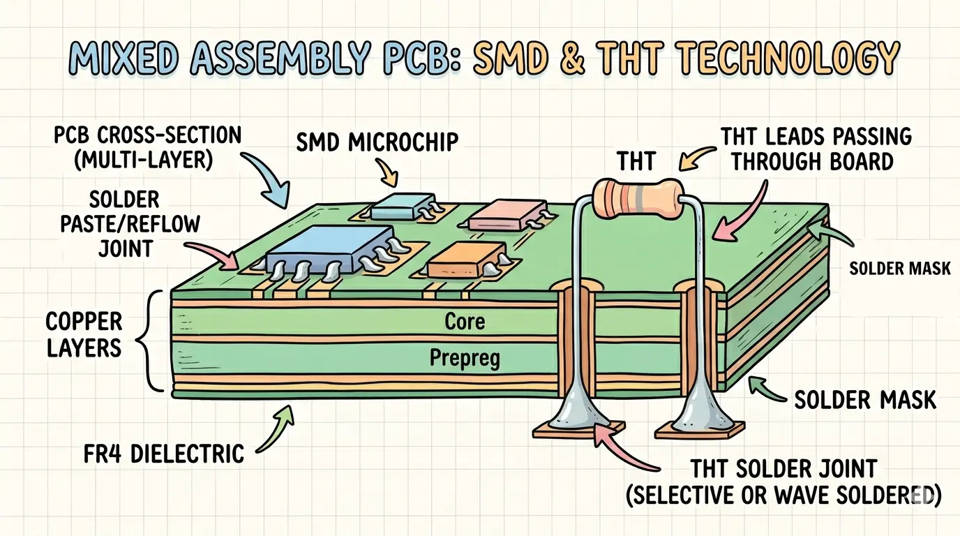
The majority of real-world production boards use both technologies. A microcontroller might use a BGA package (SMT) while its USB connector and power supply capacitors are through-hole. This is called mixed assembly.
Process sequence for mixed boards:
Why it matters for quoting: Mixed boards require more process steps, which affects lead time and price. Always declare all component types in your BOM — do not list THT parts in an SMT-only quote.
This is the end-to-end production sequence every PCBA order follows. Understanding it lets you catch design issues before they become factory holds.
BOM Review → Stencil Fabrication → Solder Paste Printing
     → SMT Pick & Place → Reflow Soldering → AOI
     → THT Insertion → Wave/Selective Soldering → Final Testing
View Ultimate PCB Assembly Guide: Prototyping to Mass Production | NextPCB
Your Bill of Materials is reviewed for completeness: manufacturer part numbers (MPNs), quantities per board, approved substitutes, and RoHS compliance. The factory cross-references parts against live inventory and distributor stock (Digi-Key, Mouser, Arrow). Long-lead items or obsolete parts are flagged immediately.
Common hold reasons at this step: Missing MPNs, "any equivalent" placeholders, mismatched footprint-to-package specifications.
If you want a complete, step-by-step guide on how to prepare a BOM for PCB assembly, see: How to Prepare BOM for PCB Assembly
NextPCB Rev0 Advantage: Rev0's AI-powered BOM parser reads your file in seconds, flags discrepancies, and auto-matches parts — eliminating the manual BOM review email chains that add 1–3 days to standard quotes.
Try NextPCB BOM TOOL or Get Component Sourcing with HQ-Online
A laser-cut stainless steel stencil (or electroformed stencil for fine-pitch BGAs) is produced to match your board's solder paste aperture pattern. Stencil thickness — typically 0.1 mm to 0.15 mm — is calibrated to deposit the correct volume of solder paste per pad.
Getting the stencil aperture-to-pad ratio right is critical: too little paste causes cold joints; too much causes bridging, especially on QFP and BGA devices.
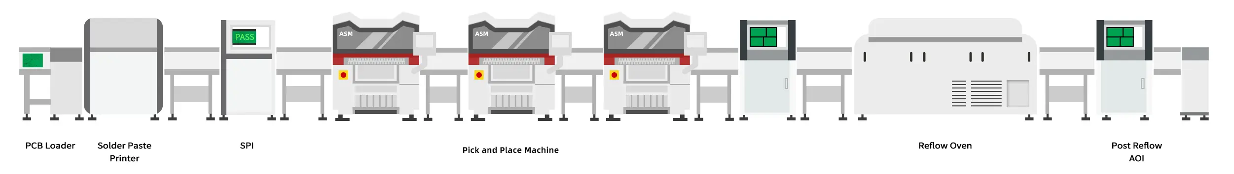
The stencil is aligned to the bare PCB on a paste printer. A squeegee blade forces solder paste (tin-silver-copper alloy suspended in flux) through the apertures onto the exposed pads. Automated paste inspection (SPI) immediately follows, measuring paste volume and offset with 3D sensors — boards with out-of-spec deposits are rejected before any component touches them.
High-speed pick-and-place machines use vacuum nozzles and vision systems to lift SMD components from tape reels or trays and place them on pasted pads with ±25 µm accuracy. Your CPL (Centroid/Pick-and-Place) file drives the machine's positional data. Placement logs are recorded for every component.
The populated board travels through a reflow oven with a precisely profiled temperature curve: preheat, soak, reflow peak (typically 235–250 °C for SAC305 alloy), and controlled cooling. The flux activates, solder paste liquefies, wets the pad and component terminal, and solidifies into a reliable intermetallic bond. Nitrogen atmosphere reflow is available for oxidation-sensitive alloys.
After reflow, every board is scanned by an AOI machine using high-resolution cameras and structured light. The system checks for: missing components, wrong components, polarity reversals, lifted leads, solder bridges, insufficient solder, and tombstoning. Defect images are logged and boards are either accepted or routed to a rework station.
Through-hole components are inserted (manually or by auto-insertion equipment) and the board passes over a wave soldering machine. For mixed boards where wave soldering would damage bottom-side SMDs, selective soldering is used — a robotic nozzle applies solder only to specified THT joints without heating the rest of the board.
Assembled boards undergo electrical testing based on your test plan. Options include:
Only boards that pass all specified tests ship. At NextPCB, free functional testing is included for qualifying orders.
Quality in PCBA is not a single pass/fail check — it is a layered system of process controls and inspection standards.
IPC-A-610, Acceptability of Electronic Assemblies, is the global standard defining what a good solder joint looks like — and what constitutes a defect. It defines three classes:
Specify your required IPC class in your order. Class 3 requires tighter solder joint geometry tolerances, additional documentation, and certified operators.
2D and 3D AOI systems inspect 100% of assembled boards after reflow. Modern systems detect defects as small as 25 µm. AOI is mandatory for all boards at NextPCB — it is not an add-on.
X-ray is required for any BGAs, QFNs, LGAs, or other bottom-terminated components where solder joints are not visible optically. The system images the solder ball lattice and detects voids, opens, shorts, and head-in-pillow defects. Available at NextPCB for complex assemblies.
For boards deployed in harsh environments (moisture, vibration, temperature extremes), conformal coating — acrylic, silicone, or polyurethane — can be applied post-assembly. NextPCB also offers IC programming, laser marking, and box build / electromechanical assembly as value-added services.
Getting an accurate quote requires three files. Missing any one of them causes delays.
| File | What It Contains | Accepted Formats | Guide |
|---|---|---|---|
| Gerber Files | PCB layer data: copper, silkscreen, solder mask, drill | .zip, .rar (RS-274X) | Gerber Files: What They Are, How to Create, View & Convert |
| BOM (Bill of Materials) | Component list: designators, MPNs, quantity, value, footprint | .xlsx, .csv, .xls | Want to Build a Killer PCBA BOM? Here's Your Step-by-Step Guide |
| CPL / Pick-and-Place | X/Y coordinates, rotation, and side for each SMD | .csv, .xlsx | How to Create a Centroid (Pick and Place) File Instantly? |
>> Read more: How to Prepare PCB Files for Assembly: Gerber, BOM, Stackup & More
This back-and-forth typically adds 3–7 days before a single board enters production.
Rev0's AI-powered platform reads your BOM on upload, cross-references 500M+ component SKUs in real time, flags issues instantly, and surfaces alternatives for out-of-stock parts — all before a human engineer touches your order.
Result: From file upload to production-ready order in minutes, not days.
Zero emails, straight to production → Rev0 PCBA Quick Prototype Service
Typical prototype lead time with Rev0:
PCBA stands for Printed Circuit Board Assembly. The term refers to the finished board after electronic components — resistors, capacitors, ICs, connectors, and other parts — have been soldered onto a bare PCB substrate. Once assembled, the board is ready to receive power and perform its designed electrical function.
A PCB is the bare substrate — copper traces and pads etched onto a dielectric material (usually FR-4), with no components. A PCBA is that same bare board after all components have been mounted and soldered. Think of a PCB as a blank circuit map and a PCBA as the complete, functional circuit. You cannot power a bare PCB and expect it to do anything; you can power a PCBA.
Prototype PCBA typically takes 5–10 business days from order confirmation to shipment, depending on board complexity and component lead times. Simple boards with all components in stock can qualify for expedited service (3–5 days). High-mix, high-complexity boards with BGAs, fine-pitch QFPs, or long-lead components take longer. Mass production schedules are quoted separately based on volume.
Three files are required for any PCBA order:
Without all three, your order cannot enter production. If you are missing the CPL file, it can sometimes be generated from your EDA tool (KiCad, Altium, Eagle) before upload.
Whether you're validating a prototype or scaling to production, NextPCB's assembly line handles everything from 1-piece engineering samples to 100,000+ unit runs — with IPC-A-610 Class 2 quality inspection standard on every order.
Straight to production.
→ Get Your PCBA Instant Quote with NextPCB → Try Ultra-Fast PCBA Prototypign with NextPCB
Want to go deeper? Read our Ultimate PCB Assembly Guide: Prototyping to Mass Production → for a comprehensive breakdown of DFM/DFA, consignment vs. turnkey supply models, and factory selection criteria.
Still, need help? Contact Us: support@nextpcb.com
Need a PCB or PCBA quote? Quote now


 Surface

