



Lolly Zheng- Sales Account Manager at NextPCB.com

 NextPCB Capabilities
Printed Circuit Boards
NextPCB Capabilities
Printed Circuit Boards
 PCB Assembly
 Layer Buildup
 SMD-Stencils
 PCB Design-Aid & Layout
 Mechanics
 Quality
 Drills & Throughplating
 Factory & Certificate
 PCB Assembly Factory Show
Certificate
PCB Assembly Factory Show
Certificate

Support Team
Feedback:
support@nextpcb.com


Table of Contents
A microvia is a very small plated hole, typically ≤150 µm (0.15 mm) in diameter, used to connect a single dielectric layer to the adjacent conductive layer in a High-Density Interconnect (HDI) PCB. Unlike a mechanically drilled through-hole or blind/buried via, a microvia is almost always formed with a laser rather than a mechanical drill bit, which is what allows it to be drilled so small and so precisely.
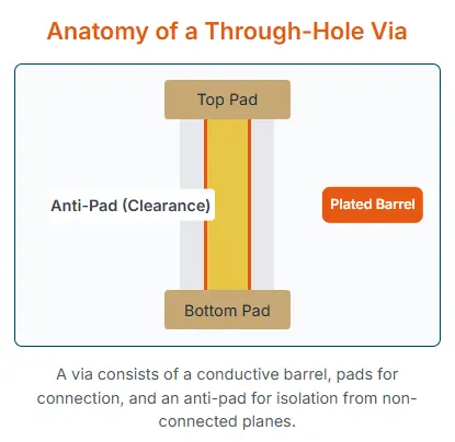
A microvia consists of three basic elements, the same as any plated via: a copper barrel that carries the electrical connection, a capture pad on the layer being connected, and, where relevant, an anti-pad clearance on any reference plane it passes through. The key difference is scale and depth: because a microvia only ever spans one dielectric layer (never the full board thickness), its aspect ratio stays low even at a tiny diameter, which is precisely what makes it manufacturable at such fine geometry.
Microvias are the enabling technology behind HDI PCBs. Without them, fine-pitch BGA packages, wearable electronics, and 5G RF modules simply could not be routed at their required density using conventional through-hole or blind/buried via technology.
Once a design needs more than one layer of microvias to reach an inner layer, the designer has to decide how successive microvia layers are arranged relative to each other. This choice has a direct impact on routing density, reliability, and cost.
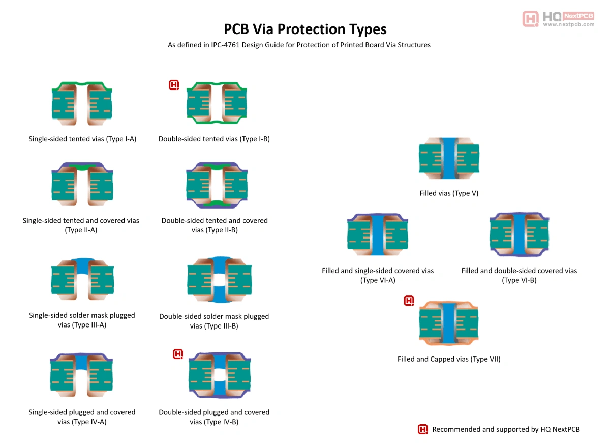
Whether a microvia needs to be filled, capped, or simply plated-and-tented is governed by IPC-4761, and the correct classification depends entirely on which of the three stacking approaches above is used.
Microvia layer count is what defines an HDI board's official classification. Understanding this is essential before sending a design to a fabricator, since quoting and DFM checks are built around these categories:
Each additional microvia layer adds a full sequential lamination-drill-plate cycle to the manufacturing process, which is the main reason cost rises steeply as you move from 1+N+1 toward Any-Layer. NextPCB's advanced manufacturing line supports up to HDI III designs and Any-Layer HDI (ELIC) on boards up to 32 layers, per its Advanced PCB Manufacturing Capabilities.
For a broader framework on deciding whether a design needs this level of via complexity at all, see: High-Speed Stackups for HDI PCBs , Multilayer PCB Design Fundamentals, and Common HDI Stackup Types (1+N+1, 2+N+2 and More).
Microvia fabrication is a fundamentally different process from mechanical via drilling, built around laser systems rather than drill bits. The typical sequence is:
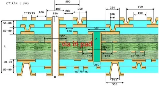
This build-up-and-drill sequence is repeated once per microvia layer, which is why HDI stackup classification (Section 3) tracks so closely with process cost and lead time.
Microvia design is governed primarily by IPC-2226 (Design Standard for HDI PCBs) and IPC-6012 (Qualification and Performance Specification), which define the manufacturing and reliability limits a design must respect:
Verified NextPCB Microvia Manufacturing Capability — the figures below are published production specifications, not general industry estimates, and confirm the design rules above at NextPCB's own facility:
| Parameter | NextPCB Capability |
|---|---|
| Min. Laser-Drilled Microvia Diameter | 0.075 mm (3 mil) |
| Microvia Aspect Ratio | Max 0.8:1 to 1:1 |
| Standard Through-Hole Aspect Ratio (for comparison) | Up to 20:1 |
| Min. Trace Width / Spacing (HDI) | 2.0 mil / 2.0 mil (0.05 mm) |
| Registration Tolerance | ±2 mil |
| Via Fill Technology | Conductive / Non-Conductive Resin + Plated Over |
| HDI Structures Supported | Up to HDI III designs, Any-Layer HDI (ELIC), up to 32 layers |
| Reliability Compliance | IPC-6012 Class 3 |
Source: Advanced PCB Manufacturing Capabilities. The 0.075 mm minimum laser-drill figure is also confirmed by NextPCB's internal drilling capability chart, which lists laser-drilled round holes at 0.075–0.15 mm, with mechanical drilling used above that range for cost reasons. Registration tolerance for laser-drilled microvias (±2 mil, roughly ±0.05 mm) is noticeably tighter than the ±0.075 mm position tolerance typical of standard mechanical drilling, which is a direct result of the laser process referenced in Section 4. These numbers are current production specifications, not a substitute for a project-specific DFM review — always confirm exact limits for a given stackup before finalizing a design.
Because microvias are so small and sit close to the board surface, they fail differently than larger through-hole or blind/buried vias. The most common failure modes are:
Mitigating these risks in practice comes down to respecting the aspect ratio and stacking limits in Section 5, specifying the correct IPC-4761 fill/cap class for the application, and requesting microsection reports from the fabricator on new stackups before committing to volume production.
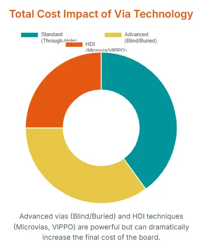
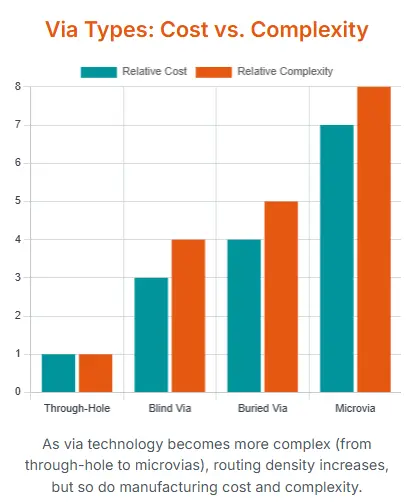
Microvia cost is driven by three factors that compound with each other:
The most effective DFM lever available to a designer is choosing the lowest HDI classification and the least aggressive microvia stacking that still meets the routing requirement — over-specifying Any-Layer or fully stacked microvias when staggered 1+N+1 would route the same design is one of the most common sources of unnecessary cost in HDI projects.
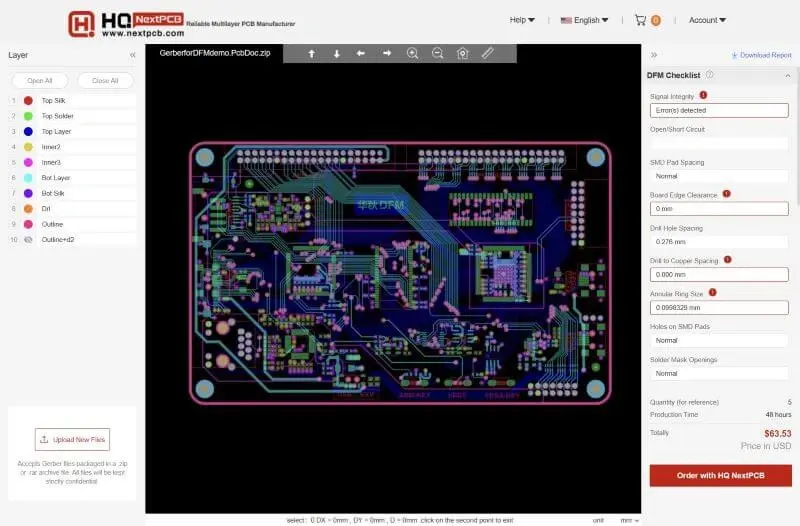
Upload your Gerber files and HQDFM will flag microvia aspect ratio, stacking, and pad size issues automatically — no sign-up required. For a full side-by-side of standard vs. advanced fabrication (layer count, materials, cost, and lead time), see Advanced PCB Manufacturing Capabilities.
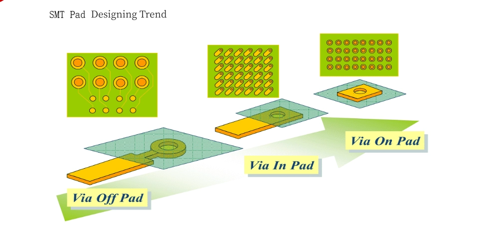
Microvias are found wherever routing density is the primary constraint rather than raw current or voltage handling:
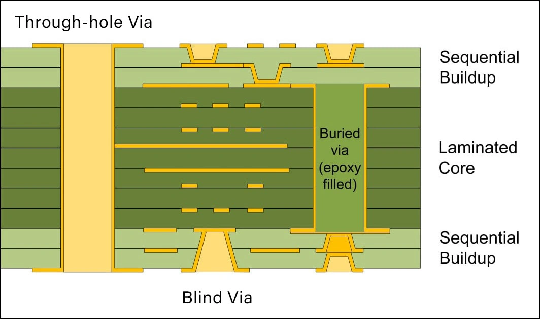
| Via Type | Spans | Drilling Method | Typical Diameter | Best For |
|---|---|---|---|---|
| Through-Hole | Entire board | Mechanical | ≥0.2 mm | Structural strength, low cost, THT components |
| Blind Via | Outer layer to inner layer | Mechanical or laser | 0.15–0.3 mm | Freeing inner-layer routing space |
| Buried Via | Inner layer to inner layer | Mechanical | 0.15–0.3 mm | Isolated internal high-speed routing |
| Microvia | Single dielectric layer only | Laser (CO²/UV) | ≤0.15 mm | Fine-pitch BGA fanout, Any-Layer HDI |
The core distinction is simple: blind and buried vias can span multiple layers using mechanical drilling, while a microvia by definition spans exactly one dielectric layer and is laser drilled. For a full breakdown of when blind vias are preferable to buried vias (and vice versa), see: Blind Vias and Buried Vias: What Is the Difference in PCB? For guidance on deciding whether your design needs any of these advanced via types at all versus a simpler through-hole approach, see: Back-Drill vs. Blind/Buried Vias: Cost, Signal Integrity, and Manufacturing Scalability.
Use our free PCB Via Current Calculator to estimate current-carrying capacity, resistance, voltage drop, and power loss — for both through-hole and buried/blind vias — based on the IPC-2221 conductor model.
Industry practice generally defines a microvia as ≤150 µm (0.15 mm) in diameter. Holes larger than this are typically classified as blind vias even if laser-drilled, since they no longer fall under the IPC-2226 microvia aspect ratio rules.
Yes, when kept within an aspect ratio of 0.8:1 to 1:1 and manufactured to IPC-6012 Class 3 HDI qualification standards. The majority of microvia field failures trace back to over-aggressive stacking or aspect ratios pushed beyond the fabricator's proven process window, not the technology itself.
There is no fixed multiplier — cost scales with the number of sequential microvia layers in the stackup and whether fill/cap is required, not with the microvia technology in isolation. A single 1+N+1 microvia layer typically adds a modest premium over a conventional multilayer board; an Any-Layer HDI stackup with multiple sequential lamination cycles can cost several times more.
Yes, but each stacked microvia must be filled and capped with copper before the next layer is drilled on top of it, or the stack will not survive lamination. Staggered microvias avoid this requirement at the cost of slightly more board area.
In production practice, yes. Mechanical drilling cannot reliably achieve the sub-150 µm diameters and tight position tolerance that microvia design rules require, which is why laser drilling (CO² or UV) is the standard process across the industry.
Upload Your HDI Design & Get Microvia DFM Review
Upload File & Quote Try HQDFM Online without Sign-Up

Still, need help? Contact Us: support@nextpcb.com
Need a PCB or PCBA quote? Quote now

