

 NextPCB Capabilities
 PCB Assembly
 Layer Buildup
 SMD-Stencils
 PCB Design-Aid & Layout
 Mechanics
 Surface
 Quality
 Drills & Throughplating
 Factory & Certificate


What is the IoT ?
The IoT refers to a technological system that interconnects various devices, sensors, and systems via the internet, enabling data collection, transmission, and intelligent analysis. IoT devices can collect environmental, equipment, and user data in real time, and make intelligent decisions through cloud-based or local analysis. In short, IoT connects various devices, sensors, and systems through a network to achieve data collection, transmission, analysis, and decision-making. A typical IoT device often includes the following modules:
- Sensing and Sampling: temperature, vibration, humidity, position, heart rate / blood oxygen, etc.
- Control and Processing: MCU/SoC responsible for data acquisition, filtering, protocol handling, and application logic.
- Communication Module: Wi-Fi, Bluetooth, LoRa, 5G, Cat-M1, NB-IoT, etc.
- Power Supply and Management: powered by battery or adapter, requiring stability under different load conditions.
- Electromagnetic Compatibility and Reliability: interference resistance, moisture resistance, vibration resistance, and temperature stress resistance.
Many seemingly "software-level" issues can ultimately be traced back to power integrity, signal integrity, PCB manufacturing, and material selection. Therefore, understanding the application scenario is not just for writing requirement documents, but for determining the PCB stack-up, process route, and testing strategy.
2. IoT Application Scenarios and Their Underlying PCB Architectures
With such outstanding data acquisition and connectivity capabilities, IoT is widely used in home, city, industrial, medical, agricultural, and other fields.
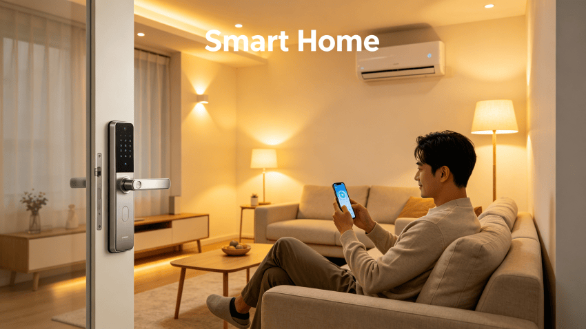
2.1 Iot Application in Smart Home: Miniaturization Priority, HDI Becomes a Common Choice
Smart home is the IoT application scenario closest to daily life. Through devices such as smart lighting, smart air conditioners, smart locks, and smart security systems, users can achieve remote control and automated management. For example, when no one is at home, smart lighting can turn off automatically, smart air conditioners can adjust temperature based on room conditions, and smart locks can remotely manage home security. This not only improves convenience but also significantly saves energy.
Smart locks, small gateways, smart sensors, etc., often face the same reality: limited space. A single device often needs to accommodate an MCU, RF module, multiple sensors, and power management simultaneously. If traditional through-hole or conventional routing approaches are still used, the number of routing layers and board area can quickly become uneconomical.
Consequently, many consumer-grade solutions lean toward HDI : for instance, using 1+N+1 or 2+N+2 structures to achieve higher interconnect density within limited layers. From an engineering perspective, the real concern is not whether to use HDI, but whether the manufacturing details can keep pace with the design density. As pin pitches shrink, the stacking of blind/buried vias, laser vias, and the copper filling process will all impact final quality.
Points to Watch
- If a three stage HDI (3+N+3) is chosen for cost reasons, but laser via stacking and copper filling are not well controlled, microcrack risks may appear after reflow soldering or thermal cycling.
- The alignment accuracy of solder mask openings affects soldering reliability; meanwhile, trace width and spacing should leave margin within mass-production capability.
In other words, smart home devices are not "the denser, the better", but should achieve miniaturization within a process window that ensures manufacturability, solderability, and long-term operation.
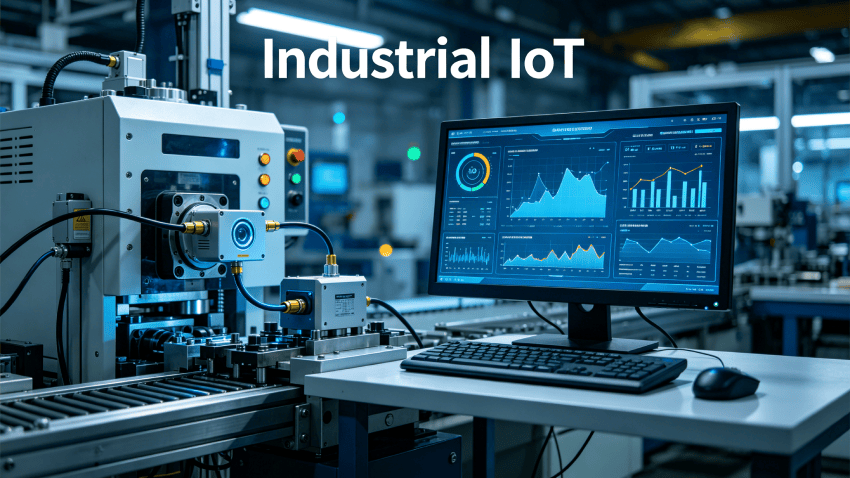
2.2 Industrial IoT (IIoT): Reliability Matters More in Extreme Environments
In the industrial sector, the Industrial Internet of Things (IIoT) enables equipment status monitoring, production process optimization, and predictive maintenance. Sensors collect real-time operational data to analyze potential faults, allowing for preemptive repairs and preventing production downtime. Additionally, IoT optimizes supply chains and inventory management, improving operational efficiency and reducing costs.
A common constraint in industrial sites is the long-term impact of temperature, humidity, and vibration, especially for sensors located near machinery and motors. Predictive maintenance often relies on the stable acquisition of extremely weak signals, which requires the PCB to be more meticulously designed for noise suppression, impedance consistency, and conductive reliability.
In these scenarios, "usability" is typically broken down into several engineering metrics:
- Integrity and stability of the signal path.
- Interference management for power and ground planes.
- Endurance of manufacturing processes and materials.
- Connection reliability (avoiding fatigue failure under long-term vibration).
Engineering Implementation and Validation Strategies
- Tight Impedance Control: Requires stricter impedance tolerance control to prevent minor deviations from amplifying into system failures.
- High-Precision Continuity Testing: Utilizes testing methods closer to real failure mechanisms (such as open/short circuit and resistance consistency verification) to screen for subtle anomalies.
- Material Selection: High-Tg (Glass Transition Temperature) materials are prioritized to reduce the risk of interlaminar stress.
- Stress Validation: Comprehensive validation under conditions like thermal cycling and thermal shock ensures that reliability is not just "sample-deep" but covers actual field conditions.
The challenge of industrial projects is often this: a prototype that works does not guarantee mass production consistency, and a device that works in the field initially may not remain reliable long-term. Therefore, PCB design and testing must be established around failure mechanisms rather than just functional power-on tests.
Case Study:
An Industrial IoT vibration sensor prototype used a standard 6-layer PCB but suffered from fragmented ground planes and RF instability. By upgrading to an 8-layer HDI (2+N+2) structure, optimizing the stackup, adding dedicated ground planes, and implementing VIPPO (Via-In-Pad Plated Over) technology, the design passed EMC testing on the first attempt, and the mass production First Pass Yield (FPY) reached 98.5%.
2.3 IoT Application in Smart Cities: RF and Signal Integrity as the Foundation
Smart cities utilize IoT technology to optimize urban management and public services. Intelligent transportation systems automatically adjust traffic light timing based on real-time road condition data to reduce congestion and improve travel efficiency. Smart streetlights can turn on/off according to ambient light and pedestrian flow, reducing energy consumption. Waste management systems monitor bin capacity via sensors to enable efficient collection and disposal. IoT makes urban management smarter and more sustainable.
In smart city applications such as streetlight control, signal acquisition, and wireless monitoring for telemedicine, "communication reliability" becomes the top priority. Wi-Fi, 5G, Cat-M1, NB-IoT, etc., all rely on RF links. However, RF issues are often not single-point failures but result from the coupling between PCB electromagnetic behavior and routing.
Engineering Logic for RF Optimization
- Dielectric loss and dielectric parameters (Df, Dk) affect high-frequency transmission quality.
- A common practical approach is to adopt a hybrid PCB stack-up: using more suitable high-performance materials in RF-related areas while keeping other areas cost-effective.
- Grounding and structural details around the antenna area impact EMI performance and radiation characteristics. The density and placement of stitching vias / ground vias directly affect the ground return path and shielding effectiveness.
For such projects, engineering needs a "reproducible design constraint" and a closed loop of "DFM/EMC/antenna consistency", rather than merely pursuing a high score in a simulation curve.

2.4 IoT Application in Healthcare: Weak Signal Acquisition and High Integration Challenges
The application of IoT in the healthcare sector is becoming increasingly widespread. Wearable devices, smart pillboxes, and remote monitoring systems can collect patients' heart rate, blood pressure, and blood glucose data in real-time, automatically uploading it to the cloud for physician analysis. This data-driven medical model enhances medical efficiency and improves patient care experiences while enabling telehealth services, which are particularly suitable for aging populations and remote areas.
Medical IoT devices (such as wearable heart rate monitors and remote monitoring systems) require not only stable communication but also have stringent requirements for weak analog signal integrity and human-body coupling environments. The core logic of their PCB design lies in high-precision signal extraction and reliability within extreme space constraints.
Engineering Logic of Medical IoT
- Ultra-low Power Consumption and Power Integrity (PI): Medical sensors typically operate at the microvolt (μV) level. The PCB must employ multi-stage power domain isolation to prevent digital switching noise from contaminating the Analog Front-End (AFE), ensuring an absolutely pure ADC sampling reference to avoid uploading diagnostic errors.
- HDI and Rigid-Flex PCBs: To adapt to human body contours and miniaturization needs, medical PCBs often utilize HDI blind/buried vias and Rigid-Flex boards. Engineering Point: In the flex area, hatched ground copper pours should be used to balance impedance control with mechanical anti-fatigue performance.
- Human Body Shielding and Electromagnetic Susceptibility (EMS): The human body is a complex electromagnetic environment that significantly shifts antenna frequencies. Designs must include impedance pre-compensation for frequency shifts caused by body proximity and integrate high-grade TVS arrays within compact spaces to resist Electrostatic Discharge (ESD) interference in medical environments.
- Absolute Analog-Digital Isolation: Critical signal lines require shielding (guard traces). Utilizing dense micro-vias to form a "Faraday cage-like" shielding structure strictly controls return paths and minimizes induced noise.

2.5 IoT Application in Agricultural: Low Power and Ionic Contamination Control
Smart agriculture utilizes IoT technology to enhance agricultural production efficiency. Soil moisture sensors, greenhouse environmental monitoring systems, and livestock management equipment enable precision irrigation, environmental regulation, and health monitoring. Through data-driven decision-making, farmers can scientifically manage fields, conserve water resources, and improve crop yield and quality.
The core constraint in agricultural scenarios is often not performance, but battery life and long-term stability. Sensors may be deployed in remote areas where battery maintenance costs are high; many solutions aim for multi-year operation.
This brings PCB issues down to a very "granular" level:
- Leakage Current and Reliability: Electrochemical Migration (ECM) and surface contamination become direct enemies of battery life.
- Environmental Impact: Humid environments amplify the effects of processing residues. If surface ionic contamination is not strictly controlled, micro-shorts may occur, accelerating battery depletion.
- Cleanliness and Surface Finishes: In low-power applications, cleanliness and the choice of surface finish are as critical as the circuit design itself. For example, using specialized surface finishes like ENEPIG (Electroless Nickel Electroless Palladium Immersion Gold) can provide a better balance of soldering reliability and surface flatness, while also helping to reduce energy consumption caused by contact resistance.
Challenges and Future Development Trends of IoT
Despite its broad application prospects, the widespread adoption of IoT remains constrained by the following factors:
- Data Security and Privacy: The interconnection of a large number of devices and data increases the risk of information leakage.
- Standardization and Interoperability: Compatibility between devices from different vendors still needs improvement.
- High Initial Investment: Deploying an IoT system requires upfront investment in devices, networks, and analytics platforms.
As technology matures, 5G networks become widespread, and artificial intelligence becomes deeply integrated, the future development of IoT will trend in the following directions:
- Deep Integration of AI and IoT: Enabling automated decision-making and intelligent optimization to improve system efficiency.
- Proliferation of Smart Cities and Smart Factories: Further improving the efficiency of urban governance and industrial production.
- 5G-Enabled Large-Scale Deployment: Leveraging the lower latency and higher reliability of 5G to drive large-scale applications.
- Green IoT Technologies: Achieving energy savings and emission reductions through intelligent means to support sustainable development.
IoT is comprehensively penetrating various domains of daily life and industry. From smart homes to smart cities, from industrial production to healthcare and modern agriculture, IoT provides intelligent solutions that improve efficiency, reduce costs, and enhance quality of life. As technology continues to evolve, IoT will keep driving society toward greater intelligence and sustainability, while data security and privacy protection remain critical issues that must be addressed.

Modern IoT PCB/HDI Technologies
1. From Standard PCB to HDI
Traditional through-hole PCBs can no longer meet the high-density requirements of modern IoT. HDI (High-Density Interconnect) technology achieves higher routing density through microvias, stacked vias, and any-layer interconnects:
- Microvias: Typically 0.1–0.15 mm in diameter, usually spanning one or two layers.
- 1+N+1 Structure: Suitable for medium-pitch BGA packages.
- 2+N+2 Structure: Ideal for SoCs where high-speed memory and RF modules coexist.
- Any-Layer HDI (ELIC): Provides maximum design freedom for ultra-compact devices like smartwatches.
2. RF Performance and Signal Integrity
Nearly all IoT devices employ wireless communication (BLE, Wi-Fi 6, LoRa, NB-IoT). High-speed digital lines are closely adjacent to sensitive RF modules, making them susceptible to EMI (Electromagnetic Interference). Solutions include:
- Impedance Control: Reducing RF trace impedance tolerance from ±10% to ±5%, which decreases signal reflection loss by approximately 1.8 dB.
- Continuous Reference Ground Planes: Avoiding ground plane fragmentation to prevent radiated emissions and certification failures.
- Hybrid Material Stackups: Using low-loss materials (e.g., Rogers 4350B or Panasonic Megtron 6) for outer layers combined with an FR-4 inner core to balance performance and cost.
3. Manufacturing Precision and Reliability
The fabrication of high-density microvia PCBs requires extreme precision:
- LDI (Laser Direct Imaging): Achieves ±25 μm alignment accuracy to prevent microvia offsets.
- Four-Wire Kelvin Testing: Detects milliohm-level resistance deviations to ensure the long-term reliability of microvias.
- Copper Balance: Utilizing thin copper layers on signal layers and balancing copper density across the stackup to reduce warpage and failure risks.
Engineer's Guidelines
|
Parameter |
Specification / Target |
|
Microvia Aspect Ratio |
Maintain ≤ 1:0.8 |
|
Solder Mask Alignment |
±25 μm accuracy |
|
Copper Balance Principle |
Ensure uniform copper distribution across layers to minimize warpage |
FAQ for IoT
Q1: Why do so many IoT devices require HDI?
Space constraint is the primary reason. Integrating an MCU, RF modules, and multiple sensors into a limited volume makes it difficult for traditional through-holes and routing densities to balance area and interconnect requirements. HDI increases routing density through microvias and buried vias while supporting interconnects near pads (Via-in-Pad, etc.), provided that the manufacturing process matches the design constraints.
Q2: How do I balance cost and performance in IoT design?
A common strategy is "localized high-spec": use high-performance materials only in the RF area while keeping non-critical regions cost-effective. Alternatively, apply higher-order HDI only in critical interconnect zones rather than utilizing the most expensive processes across the entire board. Learn more about<< PCB Design for IoT Devices: Layout, Stackup, Power & Reliability Challenges>>.
Q3: Why do devices frequently drop connections during field testing?
This requires troubleshooting Signal Integrity (SI) and RF consistency. For instance, check if impedance control meets specifications, if antenna-to-trace coupling is within tolerance, or if variations in material Dk/Df have introduced frequency shifts or loss. Many connection drops are environment-related; issues become more apparent when design and manufacturing tolerances stack up.
Q4: How are Rigid-Flex PCBs used in IoT?
They are most common in wearables or foldable form factors. Rigid-Flex reduces connector volume and allows the flexible area to handle bridging or bending requirements, while simultaneously improving vibration resistance and installation convenience.
Q5: What is the minimum trace width and spacing achievable?
Capabilities vary significantly across factories and processes. Under typical mass production conditions, 3 mil is a common stable range. Finer trace widths and spacings generally require higher-order processes (such as mSAP), which increases costs. For reference, NextPCB's minimum trace width and spacing can reach 2 mil.
Q6: How can I ensure passing FCC/CE EMC testing?
The core usually lies in systematic design of the reference ground planes and decoupling layout, rather than just adding a filter or two. Conducting a professional DFM/EMC evaluation prior to mass production can significantly reduce the probability of rework.
Conclusion
IoT is deeply penetrating daily life and industry: making homes more automated and effortless, cities more efficient and monitorable, industrial operations more predictable with less downtime, healthcare more timely and accessible, and agriculture more precise and resource-efficient.
Whether these values can truly be realized ultimately depends on the reliable delivery of hardware in real-world environments. Modern HDI PCB technology, microvia routing, impedance control, and manufacturing precision provide the foundation for IoT devices to achieve high performance, high reliability, and high yield, making smart living and industrial automation a reality.

