
 NextPCB Capabilities
Printed Circuit Boards
NextPCB Capabilities
Printed Circuit Boards
 PCB Assembly
 Layer Buildup
 SMD-Stencils
 PCB Design-Aid & Layout
 Mechanics
 Quality
 Drills & Throughplating
 Factory & Certificate
 PCB Assembly Factory Show
Certificate
PCB Assembly Factory Show
Certificate
Support Team
Feedback:
support@nextpcb.com


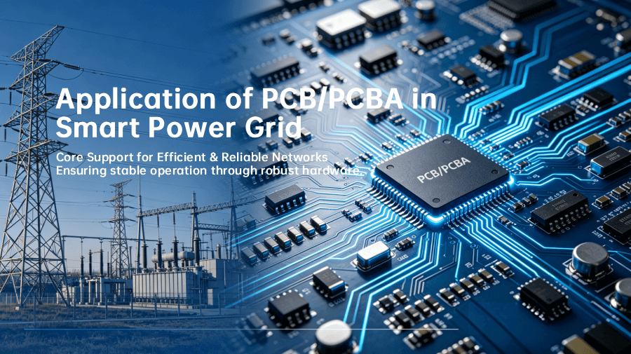
Smart grids are the core carrier of modern power systems. They integrate multiple functions—power transmission, data monitoring, and dispatch/control—to enable efficient use of electricity and reliable supply. Within this system, printed circuit boards and their assembled components serve as key parts of various electronic devices. They perform critical functions such as power conversion, signal transmission, and equipment control. Their performance and safety level directly determine the stability and security of grid operation. From protection and control/metering units in smart substations to smart electricity meters installed in homes, PCBs/PCBAs run through the entire chain of generation, transmission, distribution, and consumption. They are the hardware foundation for the digital, automated, and intelligent transformation of smart grids.
Here provides a systematic introduction to the application of PCBs/PCBAs in the power grid sector. It covers fundamental concepts, representative application scenarios, technical challenges, key design guidelines, and future development trends.
Before discussing specific applications, it is necessary to clarify the distinction between two core concepts. A printed circuit board (PCB) refers to a bare board that has undergone etching processing but has not yet had electronic components installed. It serves as the physical support for electronic components and the carrier for electrical interconnections. A printed circuit board assembly (PCBA), by contrast, is the complete circuit assembly formed on the basis of a bare PCB after electronic components are soldered, mounted, and tested. In simple terms, a PCB is the "skeleton," while a PCBA is the complete system that has the "brain" and "nerves."
In power grid applications, the control, monitoring, switching, and load-protection functions performed by PCBA make it an indispensable core component of distribution systems. Whether in smart grid equipment, industrial distribution cabinets, or new-energy power distribution systems, PCBA is a key foundation for intelligent management and safe control.
Substations serve as critical nodes within the power grid, responsible for voltage transformation and power distribution. In intelligent substations, relay protection devices act as the primary line of defense for grid security.
Taking the CPU plug-in of a relay protection and control device as an example, it utilizes high-precision analog and digital circuitry to perform data acquisition, signal amplification, and logic processing. This component is an integral part of grid protection relays, generator protection units, and automated control systems, finding extensive use in critical segments such as integrated protection devices for high-voltage switchgear.
The power supply board of microcomputer-based protection devices is equally vital. Designed in strict accordance with national standards for relay protection and power automation equipment, it is widely deployed in 10kV to 110kV distribution systems. It serves as the key component ensuring the continuous and stable operation of microcomputer protection hardware.
Smart meters are fundamental devices for intelligent management on the consumer side. By integrating a metering IC, communication module, and power-management circuitry on the PCB, smart meters enable accurate energy measurement, remote meter reading, and load monitoring. In smart grid equipment, smart meters, distribution automation nodes, edge-computing modules, transformer monitoring devices, and others all need IoT-dedicated PCBs with wireless communication capability, real-time data acquisition, and high-reliability structural design. These PCBs typically use 6 to 12 layers to isolate the power layer, signal layer, and RF channel.
In the distribution domain, intelligent controllers and communication units represent a fundamental shift from "passive protective devices" to "active network nodes." This is not merely adding another circuit board; it is equivalent to implanting a "brain" and "nerves" into circuit breakers, giving them the ability to perform real-time sensing, precise computation, autonomous decision-making, data exchange, and coordinated operation.
Taking a smart feeder module as an example, it uses PCB integration technology to highly integrate monitoring, communication, and protection functions onto a single board, completely breaking free from the constraints of traditional secondary wiring and significantly improving system reliability. The application of hot-swap technology also enables "maintenance without power interruption," which is especially important for facilities with high continuity requirements such as data centers.
As power systems evolve toward digitization and intelligence, the importance of edge-computing devices such as power gateways has become increasingly prominent. Industrial control motherboards designed specifically for edge AI deployment provide AI-accelerated computing capability and a wide range of interfaces, fully meeting the product requirements of edge-side master-control computers in smart substation intelligent monitoring platforms. Such equipment brings computing, analysis, and control capabilities down to the source where data is generated, delivering extreme real-time performance. This greatly reduces bandwidth and storage pressure while improving system reliability and autonomy.
With the large-scale grid integration of renewable energy sources such as wind power and photovoltaic (PV), demand for power-electronic equipment has surged. In areas such as PV inverters and wind power converters, high-power PCBs must carry large currents while also integrating IGBT drive and protection circuits to ensure energy conversion efficiency and safety. Renewable-energy equipment also imposes higher requirements on PCB dielectric strength (withstand voltage), heat dissipation, stability, and environmental adaptability.
Power grid equipment operates long-term in complex and harsh environments, imposing technical requirements on PCBs/PCBAs that far exceed those of conventional electronic products.
High Voltage Endurance
Substation equipment must withstand operating voltages ranging from 10kV to 110kV. According to the GB/T 16935 standard, PCB creepage distances must be ≥12mm, and interlayer insulation resistance must be maintained above 10¹³Ω over the long term. Traditional PCBs often suffer from significant insulation resistance decay in high-humidity environments.
Strong Electromagnetic Interference (EMI)
Transformers, motors, and other grid equipment generate intense electromagnetic radiation. PCBs must resist EMI across the 100–1000MHz frequency band. In substation environments, unoptimized PCBs can lead to data acquisition error rates as high as 5%, far exceeding permissible limits.
Long-Life Cycle Requirements
Power equipment typically has a design life of 15 to 20 years. PCBs must maintain stable performance through temperature cycling from -40°C to 70°C. Traditional substrates are prone to delamination and cracking under long-term thermal stress. Field tests show that smart terminals using standard PCBs reach a failure rate of 8% after five years of operation.
Extreme Temperature and Humidity
From frigid northern regions to hot and humid southern coastal areas, grid equipment faces extreme temperatures ranging from -40°C to +85°C, alongside high humidity and salt spray corrosion. These rigorous requirements must be met even during storage and transportation.
Vibration and Mechanical Shock
Mechanical vibrations during switchgear operations and shocks during transportation pose significant challenges to the soldering reliability and structural integrity of the PCB.
In high-voltage PCB design, clearance and creepage are two critical parameters. Clearance is the shortest air distance between two conductive elements; if it is insufficient, it may lead to arcing and breakdown. Creepage is the shortest distance along the surface of an insulating material, intended to prevent leakage caused by surface contamination.
During design, it is essential to strictly follow standards such as IPC-2221 or IEC 60664, setting adequate safety distances based on operating voltage and environmental conditions. When PCB space is constrained, you can increase creepage distance through slotting to ensure product safety.
In specific design practice, common safety/creepage requirements include:
Substrate selection is crucial for high-voltage, high-reliability applications. FR-4 boards with high Tg (glass transition temperature ≥ 170°C) and high CTI (comparative tracking index ≥ 600) are preferred for industrial scenarios, offering good resistance to moisture/heat and improved performance against leakage and tracking under short-circuit conditions. In severe moisture environments (e.g., chemical and metallurgical industries), select "three-proof" (triple-protection) FR-4 with water-, moisture-, and corrosion-resistant capabilities.
For copper foil thickness, high-current circuits commonly use 2 oz to 3 oz copper to improve current-carrying capacity and heat dissipation, addressing current surges caused by grid fluctuations. For more demanding power applications, metal-core substrates (aluminum-based or copper-based) and ceramic substrates are also common options.
In environments with strong electromagnetic interference, reasonable PCB layout is the core means to maintain signal integrity. Key points include:
With an optimized design, electromagnetic interference can be suppressed to below −90 dB, and the data transmission bit error rate can be controlled to below 10⁻⁹.
Power devices in grid applications generate significant heat, so effective thermal management is required. This can be achieved through wide copper traces, thermal vias, and the use of thermal pads under key heat-generating components. A reasonable layout should place power devices closer to the board edge, and combine with an external heatsink or fans for cooling. At the same time, ensure good thermal contact between power components and the heatsink by using thermal silicone grease or thermal pads.
Three-proof coating is an important guarantee for PCB reliability in power-grid applications. By applying three-proof coatings (for corrosion protection, moisture protection, and dust protection) over the PCB surface, the circuit can remain stable for long-term operation in high-dust, high-humidity, and corrosive environments. Coating thickness typically requires ≥ 50 μm, covering all component leads and solder joints. For extreme operating conditions, the entire PCBA can be further encapsulated using potting compound, filling all voids to prevent arcing and providing additional mechanical protection.
Power-grid PCBs must pass stringent reliability testing. Common test items include:
The Mean Time Between Failures (MTBF) should be ≥ 100,000 hours, which is a basic requirement for long-life operation of power equipment. In addition, the finished PCBA must undergo high-voltage insulation testing (Hi-pot test): by applying a test voltage higher than the operating voltage to the board, its insulation performance and electrical safety are verified.
As the global digital transformation of energy accelerates, smart grid equipment is becoming increasingly dependent on PCB/PCBA. Across key sectors such as Ultra-High Voltage (UHV) transmission, smart distribution networks, and renewable energy integration, PCB/PCBA technology is evolving toward higher voltage tolerance, enhanced anti-interference capabilities, and extended service life.
From a macroeconomic perspective, the global PCB market reached $74.12 billion in 2025, with the energy and power sector serving as a vital and consistently growing niche. In China, the PCB market size is projected to hit 433.32 billion RMB, accounting for over 50% of the global share. Furthermore, the localization rate of high-end products is expected to surpass 30% between 2025 and 2027.
The continuous advancement of smart grid construction will undoubtedly unlock broader development opportunities for the PCB/PCBA industry. To gain a competitive edge in this deep intersection of energy and electronic technology, enterprises must focus on sustained innovation in material science, process optimization, and quality control.
Per IEC 61010-1, the required creepage depends on the Pollution Degree and Material Group (CTI). For a typical outdoor deployment (Pollution Degree 3) using CTI > 600 material, a creepage of at least 6.3mm to 8.0mm is recommended. If board space is limited, internal milling (isolation slots) is required.
CAF mitigation is achieved through three vectors: selecting a CAF-resistant resin system, maintaining a minimum 0.3mm hole-to-hole clearance, and ensuring a rigorous vacuum lamination process to eliminate micro-voids between the glass fiber and resin.
ENIG provides a superior flat surface for fine-pitch SMT components and offers significantly better corrosion resistance in harsh industrial atmospheres containing H₂S or SO₂ compared to exposed tin-lead or lead-free solder.
In HDI designs involving microvias, copper thickness is usually capped at 2oz (70μm) for inner layers to maintain etching precision. For higher current, we utilize semi-embedded busbars or reinforced thermal vias.
We design the analog front-end (AFE) with tightly matched differential impedance (100Ω ±5%) and ensure the PCB layout separates the digital domain from the power injection domain with at least a 5mm isolation bridge.
Beyond standard ICT and FCT, we recommend Highly Accelerated Life Testing (HALT) and Temperature Cycling (-40°C to +85°C). For Smart Grid applications, a Power Cycling Test under maximum load is essential to verify that thermal expansion (CTE) mismatches between the PCB and heavy power components do not lead to solder joint fatigue.
It depends on the Glass Transition Temperature (Tg). Standard FR-4 (Tg 130°C-140°C) is generally insufficient for the thermal stresses of 3-phase systems. We specify High-Tg (170°C or 180°C) materials to ensure the board maintains structural integrity during localized heating events and to provide a higher safety margin during fault conditions.
Still, need help? Contact Us: support@nextpcb.com
Need a PCB or PCBA quote? Quote now


 Surface

