NextPCB Capabilities
Printed Circuit Boards
NextPCB Capabilities
Printed Circuit Boards
 PCB Assembly
 Layer Buildup
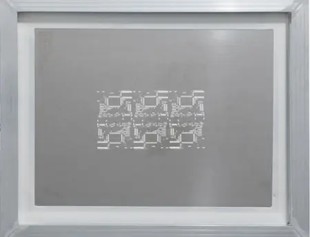
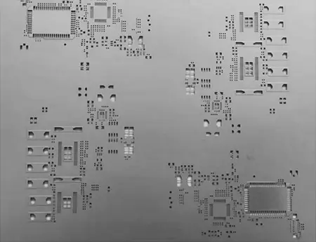
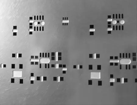
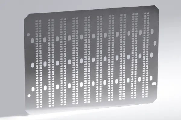
 SMD-Stencils
 PCB Design-Aid & Layout
 Mechanics
 Quality
 Drills & Throughplating
 Factory & Certificate
 PCB Assembly Factory Show
Certificate
PCB Assembly Factory Show
Certificate
Support Team
Feedback:
support@nextpcb.com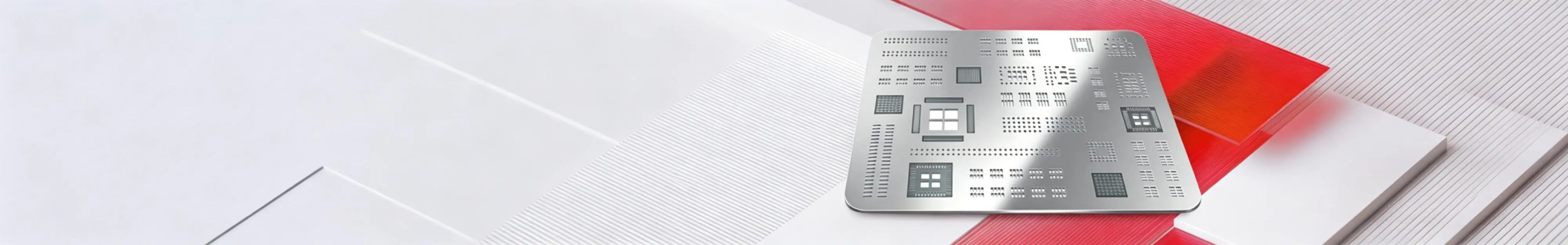
Premium Quality • Fast Turnaround • Cost-Effective.
Trusted by engineers worldwide for flawless PCBA assembly.
Precision solutions from single-layer to complex HDI boards.
Diverse stencil types to meet various SMT assembly and manufacturing requirements.
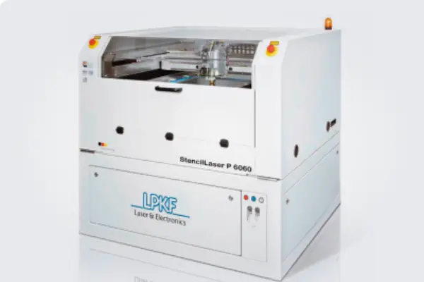
Equipped with advanced German equipment for superior processing. Ensures clean, smooth aperture walls, minimal deformation, high precision, and fast turnaround.
High tensile strength, excellent surface finish, tough and resistant to breaking. Available thicknesses range from 0.03mm to 1.0mm, with cutting accuracy up to ±0.005mm.
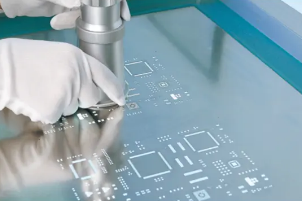
Definition & Purpose: Stencils (also known as SMT Stencils) are specialized molds used in Surface Mount Technology (SMT). Their primary function is to assist in solder paste deposition, with the goal of transferring an exact amount of solder paste to precise locations on a bare PCB.
Evolution: Stencils were originally made of mesh and were called "masks." They began as nylon (polyester) mesh, evolving into iron, copper, and finally stainless steel wire mesh for better durability. However, regardless of the mesh material, they all shared the disadvantages of poor shaping and low precision. As SMT advanced and precision requirements increased, solid stencils emerged. Influenced by material costs and manufacturing difficulty, early stencils were made of iron or copper plates. Because they were prone to rust, they were replaced by stainless steel stencils, which are the standard stencils we use today.
Background: With the prevalence of fine-pitch components like BGA and QFN, this is a top industry discussion point.
Nano Coatings (e.g., NanoSlic, EZSqueeze) reduce the friction coefficient of aperture sidewalls, ensuring cleaner solder paste release. This can improve Transfer Efficiency (TE) by 5–15%. Effectiveness is most significant for small apertures with an Area Ratio < 0.66.
Ideal for high-density boards, Lead-Free/SAC305 paste, and scenarios requiring reduced underside wiping frequency. The additional cost is typically $20–$60 per stencil; the ROI is substantial for high-volume production.
Background: Increasing demand for mixed-technology boards (large components + fine-pitch SMD) has driven the need for Step Stencils.
Step-Down: Targets fine-pitch areas (e.g., 0.4mm pitch CSP) by reducing thickness to 0.1mm to prevent bridging.
Step-Up: Targets large pads or connectors requiring higher solder volume, increasing local thickness to 0.2–0.25mm.
Design Note: Maintain a transition zone of ≥ 2mm from the step to avoid poor squeegee sealing. Laser cutting must be followed by Electropolishing or Nano Coating to treat step edges.
Background: As board density increases, solder volume control becomes more critical.
Recommended Thickness & Typical Area Ratio:
• 0402 / 0201: 0.10–0.12mm (Ratio > 0.66)
• QFN / LGA: 0.12–0.15mm (Ratio 0.70–0.80)
• BGA (0.5mm pitch): 0.12mm (Ratio ~0.75)
• General Mixed SMT: 0.15mm
• Large Pads/Connectors: 0.20mm
The industry benchmark is an Area Ratio ≥ 0.66, calculated as: Area Ratio = Aperture Area / Aperture Sidewall Area.
Background: Frequent debate in forums regarding manufacturing process selection.
Chemical Etching: Low cost and fast turnaround, but suffers from poor accuracy (tolerances > ±0.025mm) and rough sidewalls. It has largely phased out of high-precision applications.
Laser Cutting: The current mainstream standard. Offers accuracy up to ±0.005mm and smooth sidewalls. Transfer efficiency is significantly enhanced when paired with electropolishing.
New Trend: The "Triple Threat" (Laser Cut + Electropolishing + Nano Coating) is the standard for high-end stencils.
Etching Use Case: Still suitable for large apertures, low-precision requirements, or ultra-low-cost prototypes.
Background: The interface between design and manufacturing is the most common source of practical engineering queries.
File Submission: Usually requires the Paste Top (.GTP) or Paste Bottom (.GBP) layers exported directly from PCB EDA tools.
Aperture Reduction:
• BGA/QFN: Apertures are typically reduced by 10–20% of the pad area to prevent excess solder and bridging.
• 0402 and larger: Usually require no reduction, or are handled automatically by the stencil manufacturer.
Key Reminders: Verify that Gerber versions match the actual PCB revision. Specify board thickness, surface finish (HASL/ENIG), and Solder Process (Lead-free vs. Leaded) so the manufacturer can optimize apertures accordingly.
Upload your Gerber file today and experience seamless, high-quality stencil manufacturing tailored for your PCBA needs.

 Surface