
 NextPCB Capabilities
Printed Circuit Boards
NextPCB Capabilities
Printed Circuit Boards
 PCB Assembly
 Layer Buildup
 SMD-Stencils
 PCB Design-Aid & Layout
 Mechanics
 Quality
 Drills & Throughplating
 Factory & Certificate
 PCB Assembly Factory Show
Certificate
PCB Assembly Factory Show
Certificate
Support Team
Feedback:
support@nextpcb.com


The lamination process is currently the most widely used manufacturing technology for multilayer PCBs. It utilizes a subtractive process to create the circuit layers. Through a sequence of critical steps—lamination, mechanical drilling, electroless copper deposition (PTH), and copper plating—the circuits on different layers achieve electrical interconnection. Finally, the application of solder mask, surface finishes (such as HASL or ENIG), and silkscreen printing completes the manufacturing of the multilayer PCB.
Manufacturing precision directly dictates the electrical performance of the PCB. For hardware engineers, understanding the mass production capabilities of modern fabrication facilities is the first step in designing a reliable board. Below is a comprehensive table detailing the current industrial manufacturing capabilities for lamination multilayer PCBs.
Table: Common Mass Production Capability in China for Multilayer PCBs
| No. | Category | Specification | Sub-item | Mass Production Capability |
|---|---|---|---|---|
| 1 | General Specs | Base Material Type | FR-4 (Tg=140°C) FR-5 (Tg=170°C) |
|
| 2 | Max. Layer Count | 24 | ||
| 3 | Max. Copper Thickness | Outer Layer | 3 oz/ft2 | |
| Inner Layer | 3 oz/ft2 | |||
| 4 | Min. Copper Thickness | Outer Layer | 1/3 oz/ft2 | |
| Inner Layer | 1/2 oz/ft2 | |||
| 5 | Max. PCB Panel Size | 500mm (20in) × 860mm (34in) | ||
| 6 | Fabrication Capability | Min. Line Width / Line Spacing | Outer Layer | 0.1mm (4mil) / 0.1mm (4mil) |
| Inner Layer | 0.075mm (3mil) / 0.075mm (3mil) | |||
| 7 | Min. Drill Hole Size | 0.25mm (10mil) | ||
| 8 | Min. Plated Through Hole Size | 0.2mm (8mil) | ||
| 9 | Min. Annular Ring Width | Via | 0.127mm (5mil) | |
| Component Hole | 0.2mm (8mil) | |||
| 10 | Min. Solder Mask Dam Width | 0.1mm (4mil) | ||
| 11 | Min. Slot Width | ≥1mm (40mil) | ||
| 12 | Min. Legend Line Width | 0.127mm (5mil) | ||
| 13 | Min. Clearance for Negative Power/Ground Planes | ≥0.3mm (12mil) | ||
| 14 | Accuracy Specs | Layer-to-Layer Registration | ±0.127mm (5mil) | |
| 15 | Feature-to-Hole Registration | ±0.127mm (5mil) | ||
| 16 | Feature-to-Board Edge Registration | ±0.254mm (10mil) | ||
| 17 | Hole-to-Hole Registration | ±0.127mm (5mil) | ||
| 18 | Hole-to-Board Edge Registration | ±0.254mm (10mil) | ||
| 19 | Routing Profile Tolerance | ±0.1mm (4mil) | ||
| 20 | Dimensional Specs | Warpage | Double-Sided | <1.0% |
| 21 | Multi-Layer | <0.5% | ||
| 22 | Finished Board Thickness Tolerance | Thickness > 0.8mm | ±10% | |
| Thickness ≤ 0.8mm | ±0.08mm (3mil) |
A standard 4 layer pcb stackup typically contains 2 signal layers, 1 power plane (Power Layer), and 1 ground plane (Ground Layer). In terms of physical thickness distribution, a 4-layer board can adopt either an "Equal Spacing Distance Structure" or an "Unequal Spacing Distance Structure."
In an equal spacing structure, the larger dielectric thickness between the signal layer and its reference plane results in significantly higher characteristic impedance, often making it difficult to achieve standard targets such as 50Ω without increasing trace width.Conversely, with an unequal spacing structure, the impedance of the routing layers can be specifically designed and controlled to a desired target value (such as 50Ω).
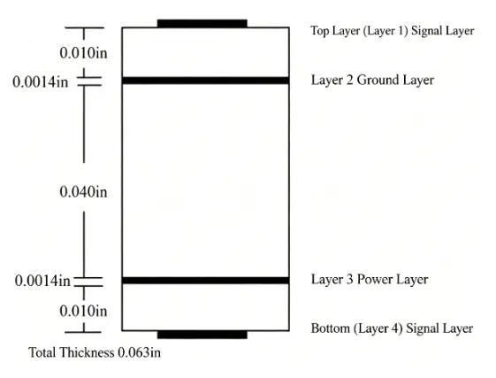
Theoretically, closely spaced power and ground layers provide a decoupling effect due to planar capacitance. However, if the physical distance between the power layer and the ground layer increases (which is common in standard 1.6mm boards), the inter-layer decoupling effect becomes very limited due to the large spacing, and cannot replace the function of discrete decoupling capacitors. Therefore, when designing circuits, it is mandatory to install adequate decoupling capacitors on the signal layer (Top Layer) near the IC power pins.
In a 4-layer board, the utilization of dedicated power and ground reference planes ensures that the physical distance from the signal layer to its reference plane is significantly smaller than in a 2-layer board. This drastically reduces RF (Radio Frequency) radiated energy. Even so, in standard configurations, the distance between the source traces and the return path can sometimes still be too large, making it difficult to perform optimal magnetic flux cancellation for RF currents generated by the circuits.
To mitigate this, engineers can route a ground trace strictly adjacent to critical signal traces on the signal layer. This provides an immediate return path for the RF return current, significantly enhancing the flux cancellation capability. An excellent design example of an unequal spacing 4-layer board consists of the following:
Read More: How to Design a 4-Layer PCB Stackup for High-Speed Digital Circuits
To ensure that the impedance does not deviate when design files are transferred to physical manufacturing, designers must base their standard pcb stackup on the actual materials used by the fabrication plant (e.g., Dielectric Constant Dk, cured thickness). NextPCB provides a wealth of board thickness options (ranging from 0.4mm to 2.5mm) and precisely defines the standard stackup for each thickness.
Below are a few prime examples extracted from the NextPCB manufacturing capabilities (For more stackup options, please refer to the Stackup Query System):
1.6mm is the industry standard thickness for the vast majority of consumer and industrial electronic products.
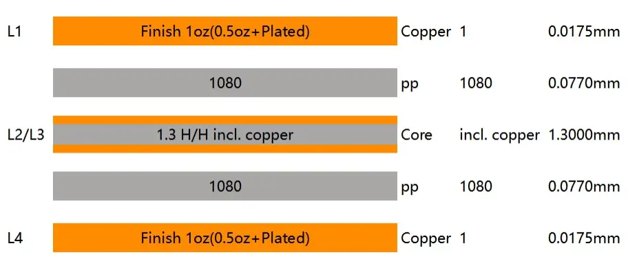
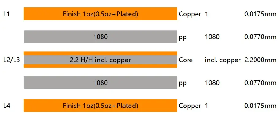
Engineering Perspective: This stackup typically utilizes a Core thickness in the range of approximately 0.8mm to 1.2mm along with 1080 Prepreg (approx. 0.077mm), depending on the fabrication process. It minimizes the L1-L2 and L4-L3 loop inductance. However, because L4's reference plane is L3 (Power), high-frequency return currents will require well-placed bypass capacitors at layer transitions to ensure continuous return paths across the thick central core.
For space-constrained IoT devices or compact modules, 0.8mm is highly recommended.
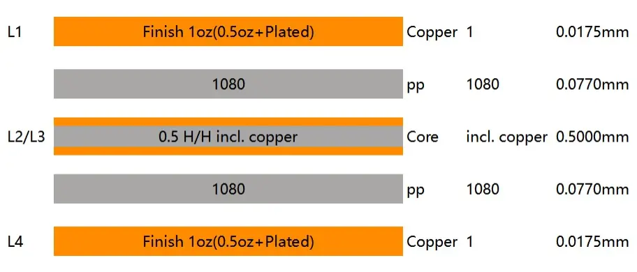
Engineering Perspective: With the central Core reduced to 0.5mm,the distributed capacitance between the power and ground planes increases significantly due to reduced spacing. This results in a lower overall Power Delivery Network (PDN) impedance compared to a 1.6mm board. It also provides a superior aspect ratio for via drilling.
In scenarios requiring high mechanical stress tolerance or deep connector insertions, thicker boards are necessary.
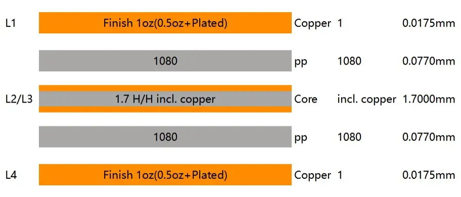
Engineering Perspective: NextPCB achieves 2.0mm and 2.5mm stackups primarily by increasing the internal Core thickness (1.7mm and 2.2mm respectively). Notably, the outer layer Prepreg remains 1080 (0.077mm). This demonstrates rigorous process control: regardless of total board thickness, maintaining consistent Prepreg specifications allows engineers to use the exact same characteristic impedance trace width rules across different projects without redesigning.
>> Rcommend reading: PCB Impedance Control Services | NextPCB
In a 4-layer board, ensuring strict impedance matching is vital for signal integrity. To prevent your traces from violating manufacturing tolerances (usually required to be within ±10%), hardware designers must abandon the habit of "guessing trace widths" and utilize precision calculation tools.
Avoid blindly trusting the default dielectric constants built into third-party EDA software (like Altium or KiCad). Different material vendors (like Shengyi or KB) have varying Er (Dk) values.
Action: Visit the NextPCB Impedance Control Stackups System.
Here, input your layer count (4 layers), target thickness, and copper weight requirements. The system will generate a standard HQDFM Stack-up report. Note down the exact thickness (H) of the PP and Core, along with their corresponding dielectric constants (Er, usually between 4.2 and 4.6).
Once you have the parameters, proceed to impedance calculation.
Action: Use the NextPCB PCB Impedance Calculator.
Tutorial:
Directly input these calculated values into your EDA software's Design Rule Check (DRC). When submitting your Gerber files to NextPCB, always check the "Impedance Control" box in the order notes; the CAM engineering team will perform final micro-adjustments to guarantee perfect performance.
>> Recommend reading: How to Achieve Controlled Impedance without Increasing Costs
Even with a perfect 4 layer pcb stackup, poor routing can degrade system performance. Keep these critical guidelines in mind:
| Verify Your 4-Layer Stackup Meets Impedance Requirements |
The most common 4-layer stackup is SIG / GND / PWR / SIG with 7628+7628 prepreg. Use NextPCB's calculator to confirm your trace widths hit your target impedance — before your PCB enters production.
Q1: Why did the fabrication plant modify my impedance trace widths during the engineering confirmation phase?
A: This is a standard industry practice. The trace widths you set in EDA software are often based on ideal dielectric constants or default thicknesses. During actual lamination, the specific Prepreg model (e.g., 1080, 2116) and resin flow rates cause minor thickness variations. To strictly hit your requested 50Ω/90Ω targets, NextPCB's CAM engineers mathematically compensate your trace widths (usually within ±20%) based on real-time material characterization. To minimize these adjustments, always use the NextPCB impedance calculator before routing.
Q2: In a standard 1.6mm 4-layer board, can I place Power and GND on the inner layers (L2/L3), and then pour solid copper polygons on L1 and L4 as additional grounds?
A: Yes, this creates a "Faraday cage" shielding effect. However, be aware of a major pain point: if you pour large copper areas on L1/L4 close to impedance-controlled microstrip lines, it inadvertently creates a Coplanar Waveguide (CPW) model. The proximity of the surface ground copper will alter the fringing capacitance and lower the trace's impedance. You must maintain a significant clearance (typically ≥ 3 times the trace width) between the trace and the poured copper, or explicitly select a "Microstrip with Coplanar Ground" model during your impedance calculations.
Q3: My 4-layer board failed EMI testing, and I noticed many high-speed signals are routed on Layer 4. Is this related to the stackup?
A: Very likely. In a standard stackup, the reference plane for L4 is L3 (Power). High-frequency return currents for L4 traces flow on the power plane. If your Power Delivery Network (PDN) lacks adequate high-frequency decoupling, or if L3 is heavily fragmented by multiple voltage islands, the return path becomes highly resistive and inductive, causing the board to radiate like an antenna. Solution: Route critical clocks and high-frequency RF signals strictly on L1 (referencing the solid L2 GND plane). If you must route on L4, ensure the power plane directly above the trace is solid and unbroken.
Q4: Is it acceptable to use a non-traditional stackup like L1(GND) - L2(Signal) - L3(Signal) - L4(Power) for internal routing?
A: While it can physically be manufactured, it is heavily discouraged from both an electrical and cost perspective. Internal routing means all high-speed lines become striplines sandwiched between planes, requiring complex via transitions just to break out the signals. Furthermore, in standard 4-layer boards, the central Core is thick (e.g., 1.2mm). Traces on L2 and L3 would be very far from their secondary reference planes, making 50-ohm impedance control nearly impossible without using impractically wide traces. Stick to the industry-standard L1(Sig)-L2(GND)-L3(Pwr)-L4(Sig) format to mitigate risks.
Q5: Why do standard 4-layer stackups always prioritize a "symmetrical" structure (e.g., using 1080 PP on both top and bottom)? Can I request an asymmetrical build?
A: PCBs are composite structures of fiberglass and epoxy resin. During the extreme heat of the lamination press (over 180°C) and subsequent cooling, thermal stresses are introduced. If the copper thickness, copper distribution, or dielectric thickness is severely asymmetrical around the central Core, the uneven release of stress will cause severe board warpage. This warpage will destroy coplanarity during SMT assembly, leading to cold soldering or tombstoning of components. NextPCB's standard pcb stackups are rigorously tested for symmetrical stress balance to guarantee high manufacturing yield and reliability.
>>> Read more: Comparison of 6-layer PCB Stack-ups
Still, need help? Contact Us: support@nextpcb.com
Need a PCB or PCBA quote? Quote now


 Surface

