Design for Manufacture (DFM) is a methodology that integrates manufacturing considerations at the product design stage. The goal is to ensure the product can be efficiently manufactured and optimized for cost and quality.
Many manufacturing challenges can be resolved or minimized with adequate insight into the intended production methods and the impact of certain design choices. Designing a product involves a tight balance between the design specification — including aesthetics, functionality and usability — and manufacturability, which ties into cost and can have a significant impact on product quality and wastage.
For electronics assemblies and PCB design, DFM equates to verifying the manufacturability and assembly of a PCB and it’s components, which can be further divided into PCB DFM and PCBA DFA for practical purposes. Through experience and training, design engineers can vastly improve efficiency by reducing prototype cycles when developing a new product. As much as 80% of production defects are caused by non-standard or poor design while 60% of a product’s total cost is determined in the design stage, highlighting DFM’s role in product success.
1.1.1. DFM Rule of 10
The DFM Rule of 10 or 10x rule highlights how the cost of fixing a design error increases exponentially the later it is caught. This can be applied to the entire product development cycle but is also apparent during a single production run.
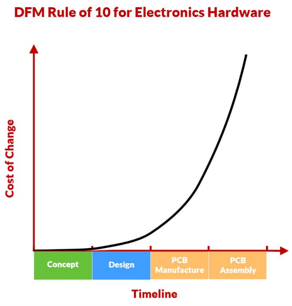
Figure 1-1: Chart illustrating the exponential increase in costs when issues are detected later in development
Despite the advanced precision of modern automated assembly systems, enterprises are still prone to encountering sub-optimal product quality and consistency. While material defects and assembly errors contribute, many issues originate from the PCB design.
DFM (Design for Manufacturability) delivers significant advantages beyond just ensuring manufacturability. By aligning design intent with manufacturing capabilities, developers gain substantial benefits—including cost reduction, enhanced efficiency, and greater product reliability through proactive issue prevention.
1.2.1. Optimizing for Production and Efficiency
A rigorous DFM inspection protocol, combined with state-of-the-art equipment, is indispensable for ensuring seamless production and end-product reliability.
If the product design does not align with the company's production capabilities and exhibits poor manufacturability, it will require greater investment of manpower, materials, and finances to achieve the desired outcomes. This can lead to delayed deliveries or even the risk of losing market share.
1.2.2. Streamlining New Product Development
When developing new products, neglecting to establish proper DFM specifications can lead to assembly issues that are only discovered in the later stages of development or even during mass production. Attempting to correct problems at this late stage will undoubtedly increase development costs and prolong production cycles.
Therefore, in addition to product functionality, integrating DFM principles is crucial throughout the new product development process. By doing so, enterprises can identify and address manufacturability challenges upfront, mitigating the risk of costly and time-consuming revisions down the line.
1.2.3. Optimizing High Density Designs
The electronics industry's demand for smaller, more powerful devices is driving PCB designs towards ever increasing density. Circuits are being pushed to feature finer and more closely-spaced traces, smaller hole diameters, advanced via technologies, and more complex structures.
This trend towards higher-density PCB designs amplifies the need for precise, comprehensive Design for Manufacturability (DFM) analysis techniques and tools to achieve first-pass success, reduce costs, and accelerate time-to-market.
1.2.4. Standardizing Documentation
Improper design or unclear fabrication guidelines can create significant challenges on the factory floor. When produced boards fail to meet requirements or need to be scrapped, the costs of rectifying these issues and the resulting impact on the production cycle can be substantial. DFM helps by standardizing technical documentation and aligning intent, particularly when it comes to PCB fabrication data, since PCB fabrication data is represented graphically which can be prone to misinterpretation.
1.2.5. Ensuring Compatibility with Automated Assembly
Surface Mount Technology (SMT) is characterized by high automation and high-speed manufacturing, relying heavily on specialized equipment. Subsequently, they have specific requirements regarding the size, shape, reference points, and component layout of the PCBs and panel to ensure compatibility. DFM can verify the panel design including checking the presence of fiducial markers and tooling margins.
1.2.6. Minimizing Non-Production Related Design Errors
Design flaws that do not directly impact manufacturability are often addressed under DFM. This is because design mistakes, even those unrelated to production, can be fatal - impacting entire batches and potentially being mistaken for manufacturing issues. Expanding DFM's scope helps mitigate these broader design risks and improve reliability in the long-term.
Since PCB fabrication and assembly are often undertaken by separate parties, even within the same company, it makes sense to align manufacturing considerations for a product with the priorities and responsibilities of the respective party i.e. bare board (PCB DFM) for fabricators, and assembly optimization (PCBA DFA) for CM partners. As such, the term DFM may mean different things to different parties.
When PCB fabricators mention DFM review, they often refer to the Design for manufacturability analysis of bare printed circuit board designs. However, for contract manufacturers and assembly houses, DFMlikely refers to PCBA Design for Assembly, that is, analyzing how the circuit board and components match and how the design may impact assembly.
In HQDFM, DFM analysis is distinctively divided into PCB DFM and PCB assembly DFA, both of which are essential to the successful production of a product. In future discussions, the term DFM refers to both PCB DFM and PCBA DFA unless otherwise mentioned.
Although most PCB fabrication and assembly providers also perform DFM/DFA review, their depth and reliability vary considerably. Typically, suppliers conduct these reviews out of necessity—primarily to verify that designs meet their manufacturing capabilities and contain sufficient documentation. Advanced suppliers may provide more thorough analyses, but since DFM/DFA checks usually occur after order submission, an in-depth review may introduce significant delays for marginal benefit. As a result, suppliers typically flag only the most critical errors.
HQDFM is a free PCB DFM analysis tool developed by NextPCB for viewing PCB manufacturing files and performing quick DFM and DFA analysis. Covering over 150 design for manufacture and assembly issues, HQDFM provides actionable insights to help users enhance reliability, reduce costs and streamline production
HQDFM takes a comprehensive approach, considering PCB manufacturability, assembly, and testing throughout the product life-cycle. By closely integrating design and manufacturing, HQDFM maximizes the chances of first-time success as products move from design to production.
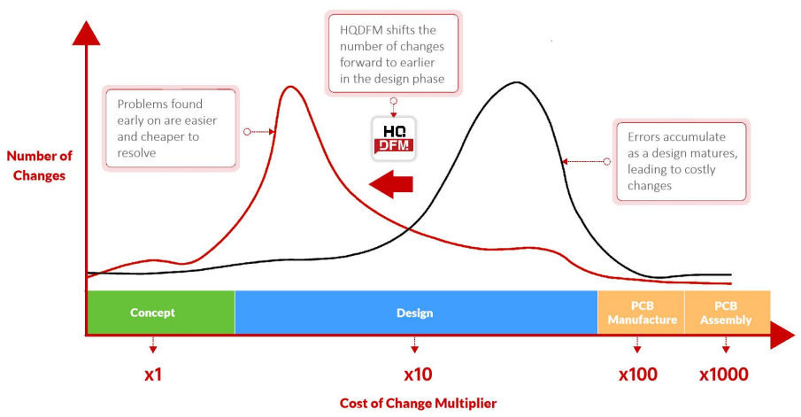
Figure 1-2: HQDFM impact on reducing development costs by detecting issues earlier in the design phase
HQDFM also provides a suite of tools for PCB designers, contract manufacturers and PCB fabrication houses to extract useful information from manufacturing data.
1.4.1. HQDFM Key Features
Gerber Viewer: Dedicated workspace for displaying PCB graphical data including navigating individual layers with zoom, pan and snap options, dimensional analysis and various viewing modes such as realisticand CAM modes.
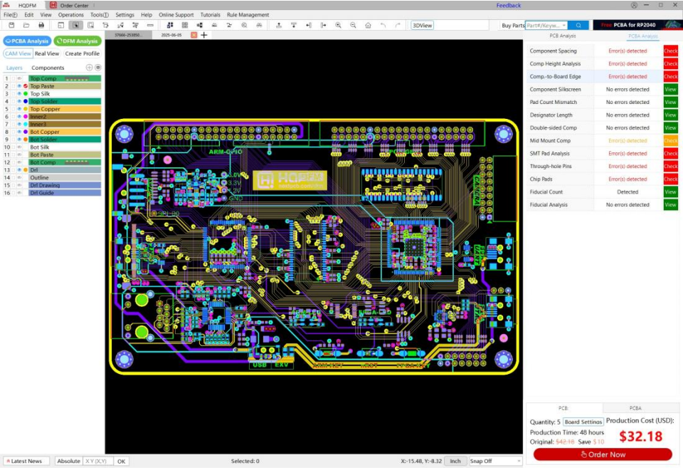
Figure 1-3: HQDFM standard Gerber viewer interface
DFM Analysis: One-click Design for Manufacture (DFM) analysis and parameter extraction for bare printed circuit board designs using HQDFM algorithms. Based on PCB production data only (Gerber, drill, ODB++).
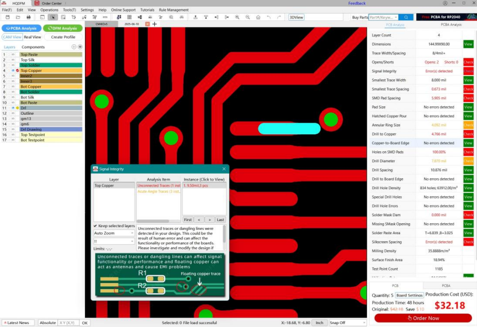
Figure 1-4: HQDFM PCB DFM analysis interface
DFA Analysis: PCBA Design for Assembly (DFA) analysis for populated electronic assemblies (including the PCB and electronic components) using HQDFM algorithms. Requires the Bill of Materials (BOM) and Centroid (pick-and-place) data in addition to PCB production data.
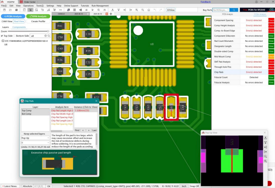
Figure 1-5: HQDFM PCBA DFA analysis interface
Footprint Checker: Quick and easy automated footprint checker covering over 6 million parts and growing.
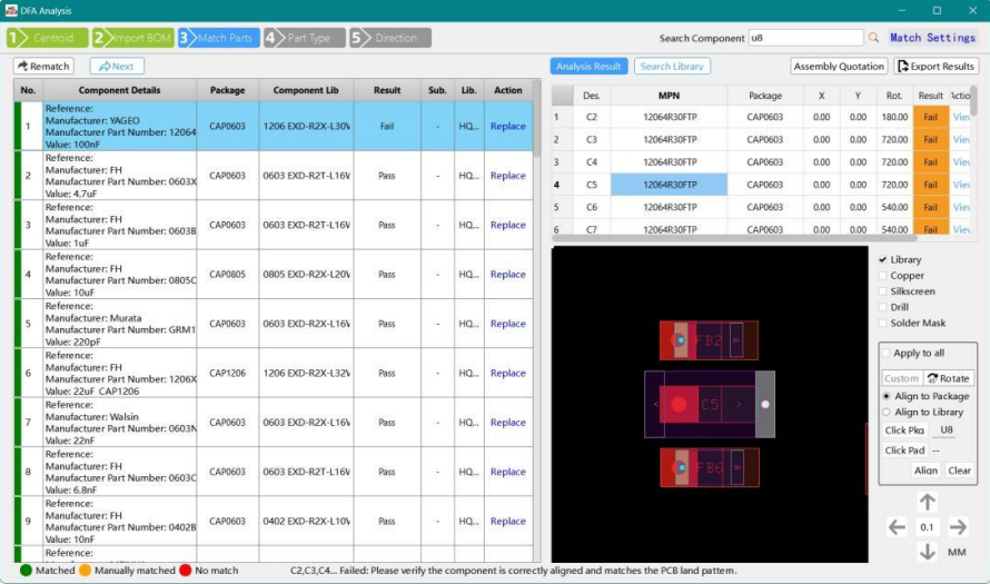
Figure 1-6: HQDFM footprint checking interface
1.4.2. HQDFM Tools
Panelization Tool: Create panelized data purely from the production files quickly and easily. Customize everything from layouts, margin widths, board spacings and add tabs, stamp holes and Fiducial marks in a single interface. Or use the Smart Panelization tool to give suggested layouts based on RawPanel Size to maximum utilization rates.
Impedance Calculator: Quickly calculate controlled impedance for multiple traces simultaneously using parameters such as trace geometry, material properties and layer stackup. HQDFM’s impedance calculator supports various trace types (single-ended, differential, co-planar) and transmission line structures including Microstrip, Embedded Microstrip, Stripline and Dual Stripline<>.
BOM Checker and Centroid File editing: Perform simple time-saving and potentially project-saving BOM checks with a single-click and edit Centroid files in a simple spreadsheet like interface with real-time visual feedback.
Compare Gerber Files/BOM Files: Never send the wrong files again with HQDFM’s Compare Gerber and BOM file tools. Track changes across versions and identify differences between after automated file operations in seconds.
And many more tools including Utilization Rate Calculator, Solder Pad Count, Routing Distance, Component Search, Net Length Calculator, Copper Area Calculator.
1.4.3. What can and can’t HQDFM do?
Can:
Open and view PCB production data. HQDFM can be used to open and navigate PCB production data including Gerber files in RS-274x, X2 and X3 format (additional X3 information is not currently utilized), Excellon NC drill files in Excellon format and ODB++ files. As PCB manufacturing data is typically graphical in nature, HQDFM also offers a graphical interface for viewing the individual layers of a PCB.
Production data is typically exported in industry standard formats (e.g. Ucamco Gerber format). However, the accuracy of the produced data depends on the accuracy of the implementation in the ECAD tool.
Likewise, different manufacturers have different interpretations of the same set of data, resulting in discrepancies and misunderstandings. By understanding how manufactures understand and use production data, designers can facilitate communication with manufacturers and avoid mistakes.
Can't:
Design PCBs - HQDFM is not a PCB design tool. HQDFM is designed to be used in conjunction with ECAD tools such as KiCad and Altium to verify the production data exported before hand-off. For most design-based errors, designers should make modifications to the original ECAD design file if possible and re-export the PCB production data and repeat analysis.
Reverse engineer PCBs i.e. Gerber to PCB file. HQDFM can only utilize the data provided. It cannot generate schematic information, ECAD design files, missing layers or auto-create Centroid (pick-and-place) data etc. Tools in HQDFM can be used to manually build centroid files, modify and export modified Gerber files and find connections using the netlist. However, these features require specialized PCB engineering knowledge and should be used with care to avoid errors.
Ensure your design is manufacturable - HQDFM cannot guarantee that 1) your design can or cannot be manufactured or 2) the fab house will not report errors (EQs or engineer questions). This can be due to a multitude of reasons:
- Each manufacturer’s requirements and standard processes vary.
- Accuracy of error reporting may depend on the quality of the provided data, which is determined by the ECAD software.
- Some aspects of a design cannot be reliably determined from the production files and 100% coverage is impossible. Like all validation tools, HQDFM helps reduce errors and streamlines their detection using the available data.
- HQDFM’s DFM and DFA analysis features are designed for rigid PCB constructions and include limited support for HDI boards. Flex, rigid-flex, other specialized board types and features are currently not supported though these may be added in the future.
HQDFM should be used in conjunction with user experience and knowledge of the design requirements and should not be used as a substitute for human experience and validation.
1.5.1. System requirements:
- a) Windows 7, Windows 10 or Windows 11 operating system
- b) At least 1.12GB of disk space
- c) Graphics card with OpenGL version 1.0 and above support
1.5.2. Installation steps:
1. Download HQDFM from NextPCB at https://www.nextpcb.com/dfm
2. Extract the contents of the zip file and double-click the installation package to start the installation wizard. If you receive a warning preventing an unrecognized app from starting, click [Run] or click [More info] then [Run anyway] on Windows 11 systems and similarly on older systems.
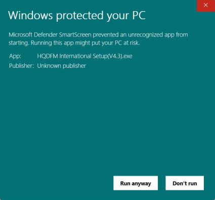
Figure 1-7: Windows 11 SmartScreen pop-up
3. The default installation path is C:\Program Files\HQDFM International which can be changed. Click [Next].
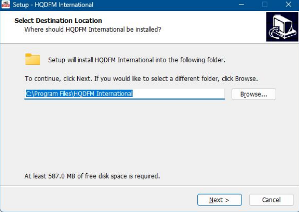
Figure 1-8: HQDFM program installation directory
4. Click [Next] to create a Start Menu shortcut in the folder indicated.
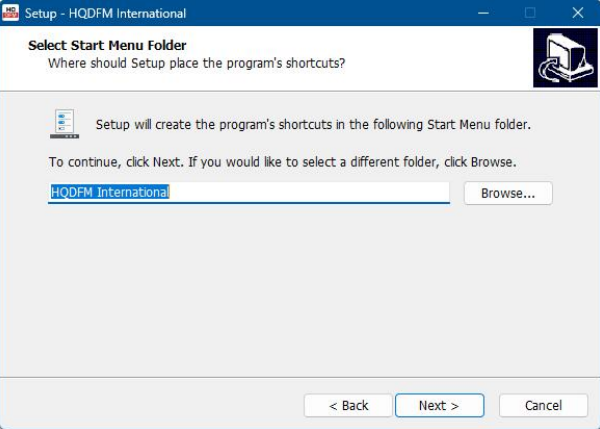
Figure 1-9: Start menu shortcut creation
5. Choose whether to create desktop and Quick Launch shortcuts then click [Next]
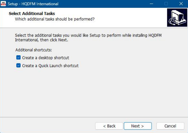
Figure 1-10: Desktop and quick launch shortcut creation
6. Confirm the install settings and click [Install] to proceed with installation.
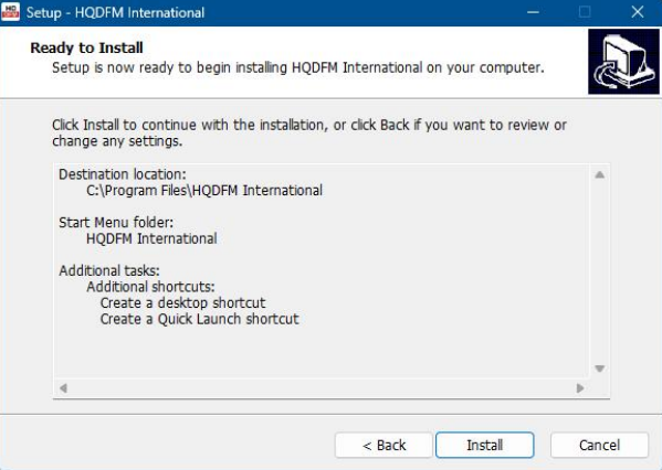
Figure 1-11: Confirming installation settings
7. Once installation is complete, click [Finish] to close the wizard and launch HQDFM.
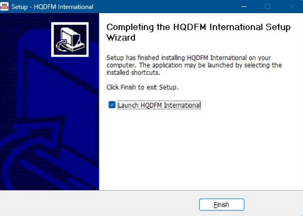
Figure 1-12: Completing installation
1.6.1. HQDFM accepts the following files for analysis:
- a) CAD files: RS-274X, X2 and X3 Gerber files, Excellon Drill files, ODB++ files and KiCad .kicad_pcb files(HQDFM version 4.6 and above only).
- b) BOM files: .xls, .xlsx Excel files and .csv text files
- c) Centroid (XY) files: .xls, .xlsx Excel files and .csv text files
1.6.2. How to open files in HQDFM
There are numerous ways of importing PCB production files into HQDFM:
- a) Click New File and browse for the files to import in the new window.
- b) Drag and drop the files from file explorer or the desktop directly.
The main workspace accepts individual file import, multi-select import and .rar and .zip archive file import.
| Menu |
Name |
Menu Shortcut |
Shortcut |
Notes |
| Menu Bar |
File |
Alt + F |
|
|
| Open |
Alt + F → O |
|
|
| New |
Alt + F → N |
|
|
| Close |
Alt + F → C |
|
|
| Save as DFM File |
Alt + F → H |
|
|
| Export Gerber Files |
Alt + F → G |
|
|
| Export ODB++ |
Alt + F → T |
|
|
| Export DFM Report |
Alt + F → R |
|
|
| Export PDF |
Alt + F → P |
|
|
| Recent |
|
|
|
| Exit |
Alt + F → X |
Ctrl + X |
|
| Edit |
Alt + E |
|
|
| Add |
Alt + E → A |
Ctrl + A |
|
| Delete |
Alt + E → D |
Delete |
|
| Move Layer/Object |
Alt + E → M |
Ctrl + D |
|
| Copy Layer/Object |
|
|
|
| Rotate Layer/Object |
Alt + E → R |
|
|
| Mirror Layer/Object |
Alt + E → I |
|
|
| Set Origin |
|
|
|
| View |
Alt + V |
|
|
| Toggle Fill Mode |
Alt + V → F |
F |
|
| Show Negative Objects |
Alt + V → N |
N |
|
| Component Display Settings |
Alt + V → Y |
Y |
|
| Component List |
Alt + V → I |
I |
|
| CAM/Real View Mode |
Alt + V → D |
D + S |
|
| Operations |
Alt + O |
|
|
| Zoom to Window |
Alt + O → R |
|
|
| Object Select |
Alt + O → F |
|
|
| Box Select |
Alt + O → E |
|
|
| Same-Layer Net Select |
Alt + O → S |
|
|
| Cross-Layer Net Select |
Alt + O → N |
|
|
| Trace Select |
Alt + O → T |
|
|
| Measure |
Alt + O → M |
Ctrl + M |
|
| Tools |
Alt + T |
|
|
| Impedance Calculator |
|
|
|
| Compare Gerber Files |
Alt + T → C |
|
|
| Panelization Tool |
Alt + T → P |
|
|
| Calculate Routing Distance |
Alt + T → R |
|
|
| Utilization Rate |
Alt + T → U |
|
|
| Count Solder Pads |
Alt + T → S |
|
|
| Compare BOM Files |
Alt + T → B |
|
|
| Find Component |
Alt + T → D |
|
|
| Compare IPC Nets |
Alt + T → N |
|
|
| Calculate Copper Area |
Alt + T → O |
|
|
| Interactive BOM |
|
|
|
| Board Settings |
|
|
|
| Library Management |
Alt + T → W |
|
|
| Create Component |
|
|
|
| Settings |
Alt + S |
|
|
| Units |
|
|
|
| General Settings |
Alt + S + J |
|
|
| Object Snap |
Alt + S → O |
|
|
| Keyboard Shortcuts |
Alt + S → |
|
|
| Rule Management |
Alt + S → C |
|
|
| Proxy |
|
|
|
| Help |
Alt + H |
|
|
| About HQDFM |
|
|
|
| Follow HQDFM |
|
|
|
| Online Support |
Alt + C |
|
|
| HQDFM Technical Support |
|
|
|
| Tutorials |
|
|
|
| Tutorial Videos |
|
|
|
| HQDFM User Manual |
|
|
|
| Actions |
DFM Analysis |
|
|
|
| Calculate PCB Size |
|
|
|
| Append File |
|
|
|
| Layer Management |
|
|
|
| Pan Left |
|
← |
|
| Pan Right |
|
→ |
|
| Pan Up |
|
↑ |
|
| Pan Down |
|
↓ |
|
| Reset View |
|
Home |
|
| Zoom In |
|
PageUp / + |
|
| Zoom Out |
|
PageDown / - |
|
| Undo |
|
Ctrl + Z |
|
| Redo |
|
Ctrl + U |
|
| Open All Layers |
|
Alt + A |
|
| Close All Layers |
|
Shift + A |
|
| Aperture List |
|
Right Mouse Button |
|
| Drill File Format |
|
Right Mouse Button |
|
| Export Layer |
|
Right Mouse Button |
|
| Measure Point-to-Point |
|
M + P |
|
| Measure Object-to-Object |
|
M + O |
|
| Measure Network-to-Network |
|
M + N |
|
| Toggle Crosshair |
|
X |
|
| Switch Working Layer |
|
D + A |
|
1.8.1. HQDFM works best with a keyboard and mouse setup.
The mouse controls are designed to help users navigate Gerber files in a quick and seamless manner independently, leaving the other hand free to activate actions via keyboard shortcuts.
Mouse Actions:
- a) Left mouse button: Select objects, double-click to select similar objects, cancel selection by clicking in blank areas in the workspace.
- b) Middle mouse button: Scroll to pan up and down, hold the middle mouse button and move the mouse forward and back to zoom in and out.
- c) Right mouse button: Right click in the workspace to bring up the command menu for easy access to common commands. Right-click and hold to pan the workspace by dragging the mouse.
Double click the desktop icon to open HQDFM and enter the main interface. The main interface consists of the menu bar and toolbar on top, the workspace in the middle, layer navigation panel on the right and the PCB and PCBA DFM checklist panel on the right. On the bottom right, you can change the units from mil to mm, change the snapping property and view the XY coordinates of the last mouse click in the workspace.
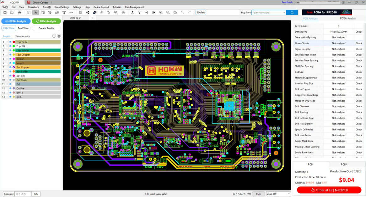
Figure 2-1: HQDFM main interface
| Menu |
File |
Edit |
View |
Operations |
Tools |
|
| Function |
Open |
Add |
Toggle Fill Mode |
Zoom to Window |
Impedance Calculator |
|
| New |
Delete |
Show Negative Objects |
Object Select |
Compare Gerber Files |
|
| Close |
Move Layer/Object |
Component Display Settings |
Box Select |
Compare BOM Files |
|
| Export Gerber/Drill |
Copy Layer/Object |
Component List |
Same-Layer Net Select |
Filter |
|
| Export ODB++ |
Rotate Layer/Object |
3D Viewer |
Cross-Layer Net Select |
Analyze > |
Compare IPC Nets |
| Export DFM Report |
Mirror Layer/Object |
CAM/Real View Mode |
Trace Select |
Calculate Copper Area |
| Export PDF |
Set Origin |
|
Measure |
Net Length Calculator |
| Recent > |
|
|
|
Assembly > |
Count Solder Pads |
| Exit |
|
|
|
Component Search |
| |
|
|
|
Export Centroid Data |
| |
|
|
|
Panelization > |
Smart Panelization |
| |
|
|
|
Panelization Tool |
| |
|
|
|
Calculate Routing Distance |
| |
|
|
|
Utilization Rate |
Figure 2-2: Menu bar options
| Manu |
Board Setting |
Settings |
Help |
Online Support |
Tutorials |
Rule Management |
| Function |
Board Settings |
Units > |
Video Tutorials |
service@nextpcb.com |
HQDFM User Manual |
Rule Management |
| |
General Settings |
HQDFM |
Tel: 0086-755-8364 3663 |
|
|
| |
Object Snap |
About us |
Phone: +86 13622941920 |
|
|
| |
Keyboard Shortcuts |
|
|
|
|
Figure 2-3: Menu bar options continued
2.2.1. File menu options
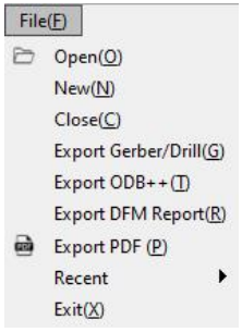
Figure 2-4: File menu
Open: Open Gerber, ODB++ or HQDFM .DFM job file
New: Create a new project. The HQDFM workspace supports opening multiple projects for enhancedconvenience and productivity.
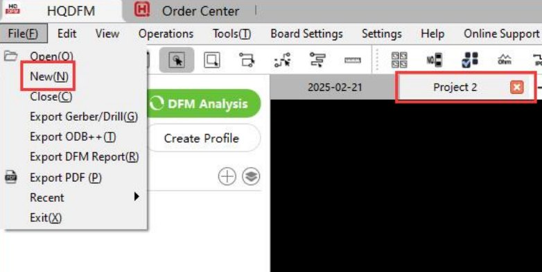
Figure 2-5: New project function
Close: Close the current job.
Export Gerber Files: Export Gerber files in the current workspace including edits made in HQDFM. This feature is currently in beta testing and may not support non-standard Gerber implementations. Please import and review the exported files again in HQDFM to ensure the files have been correctly generated.
Export ODB++ Files: Export ODB++ files for PCB manufacture; can also generate ODB++ files from Gerber format files.
Export DFM Report: Export a report containing all the results of the Design for Manufacture and Assembly analysis.
Export PDF: Customize and choose layers to be exported in PDF format. Layers can be exported overlapping or individually, mirrored, enlarged or to scale, and in color or black and white.
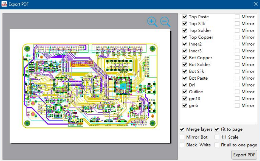
Figure 2-6: Export PDF interface
Recent: Open recently opened files; HQDFM will save the last 10 files.
Exit: Close HQDFM.
2.2.2. Edit menu functions
The edit menu contains functions for editing elements in Gerber files including adding graphical elements, rotating and mirroring objects and entire layers.
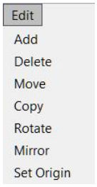
Figure 2-7: Edit menu
Add: Add lines, flashes, arcs, polygon fills and text to Gerber files.
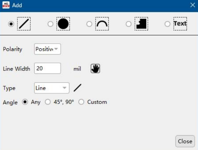
Figure 2-8: Add objects interface
a) Line: Lines for drawing traces or outlines etc. Lines can carry positive or negative attributes and can be drawn at any angle. Use the hand tool and click an existing line to copy the aperture. Rectangles can also be drawn using this tool.
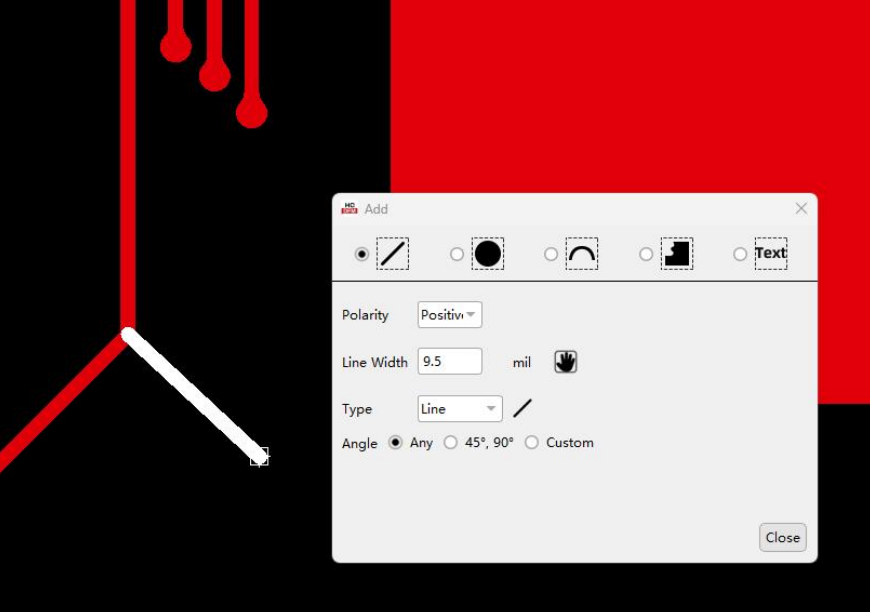
Figure 2-9: Add line interface
b) Flash: Fixed shapes for creating pad flashes. Use the hand tool to grab an existing aperture from the Gerber files. Flashes can be positive or negative. There are 24 styles to choose fromincluding oblongs, diamonds, thermals, crosshairs and rings. Flashes can be added in arrays by entering the array-matrix and spacing.
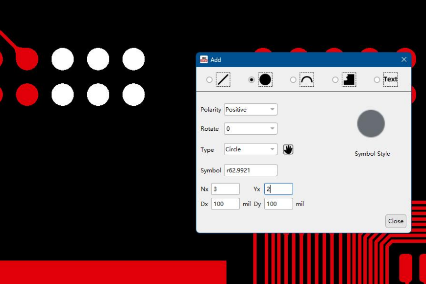
Figure 2-10: Add flash interface
The precise dimensions of each shape style can be modified, or use the hand tool to copy the aperture size of an existing flash.
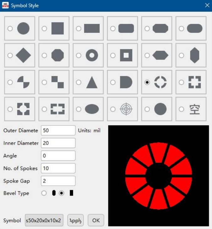
Figure 2-11: Flash styles
c) Arc: Arc types can be positive or negative. There are three methods for drawing arcs:
- Endpoints: Click the two endpoints of the arc then move the mouse away fromthe center of the two points to visualize the arc. Click again to fix the arc and press enter to commit the arc to the working layer.
- Center: Click one endpoint, then click the center of the arc circle. Follow the perimeter of the circle with the mouse and click again to create the arc of the desired length. Press enter to commit the arc to the working layer.
- Radius: Use the radius method to create arcs with a specified radius. Click on the workspace to set the arc circle origin and follow the perimeter of the circle to visualize the arc. Click again to set the arc length and press enter to commit the arc to the working layer.
Complete circles can also be created using the above three methods. Instead of clicking once and pressing enter to commit the arc, you can also double click.
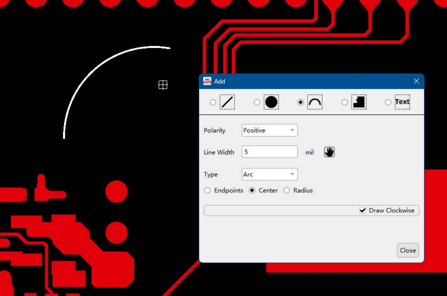
Figure 2-12: Add arc interface
d) Polygon fill: HQDFM supports the creation of rectangular or free-form filled polygons in positive and negative polarities. Draw the shape then double click or press enter to commit the shape to the working layer.
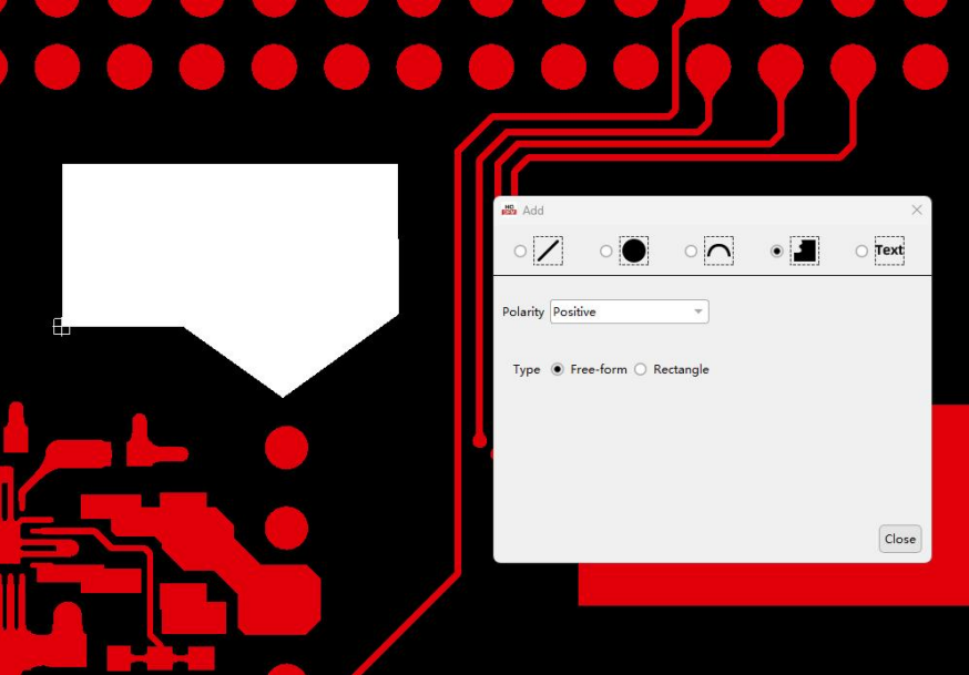
Figure 2-13: Add polygon fill interface
e) Text: Text can be entered with positive or negative polarity, at an angle or mirrored. Modify the text font, size and line width in the dialog then click on the workspace to print the text on the working layer. The hand tool can be used to grab an existing aperture size. The ideal text height to width ratiois 1.5: 1
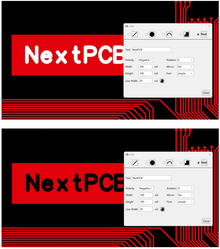
Figure 2-14: Add text interface
Delete: Remove objects by selecting the element or elements and clicking delete, or press the delete key on the keyboard. If no specific element is selected, the entire layer will be deleted.
Move: The move function can be used to move or align objects, layers and groups of objects. Select multiple working layers by checking the boxes in the layer manager to move the contents of different layers together.
a) Single object: Move/align a single object. Select the object then click the Move function from the menu bar or by right clicking. Click to set the anchor point, move the mouse to the new location and click again to move the object.
b) Layer: Align an entire layer that is misaligned with other layers. Click the Move function and find a common point shared by the two layers e.g. a pad. Click the point on the working layer, then click the corresponding point on the layer you want to align to. The working layer will move to the new location. Use snap options to make sure the layers align perfectly.
c) Selection: Select the objects to move with the window selection tool, click the anchor point, move the cursor to the new location and click again to move the objects. Check multiple layers to select the contents of more than one layer.
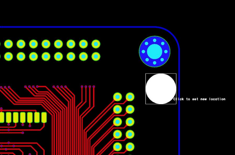
Figure 2-15: Move function
Rotate: Select the objects to rotate and click the rotate function. If no objects are selected, the entire working layer will be rotated. Select the origin and the angle of rotation. Click apply to rotate the object/layer and click OK to confirm. A custom origin can be entered.
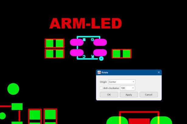
Figure 2-16: Rotate dialog
Mirror: Select the objects to mirror and click the Mirror function. If no objects are selected, the entire working layer will be mirrored.
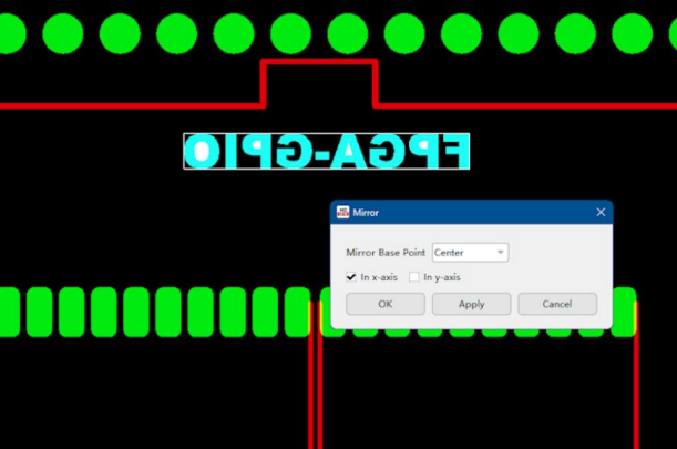
Figure 2-17: Mirror dialog
2.2.3. View menu functions
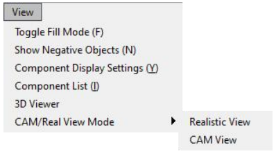
Figure 2-18: View menu
Toggle Fill Mode: Toggle between normal, outline and skeleton Gerber fill modes.
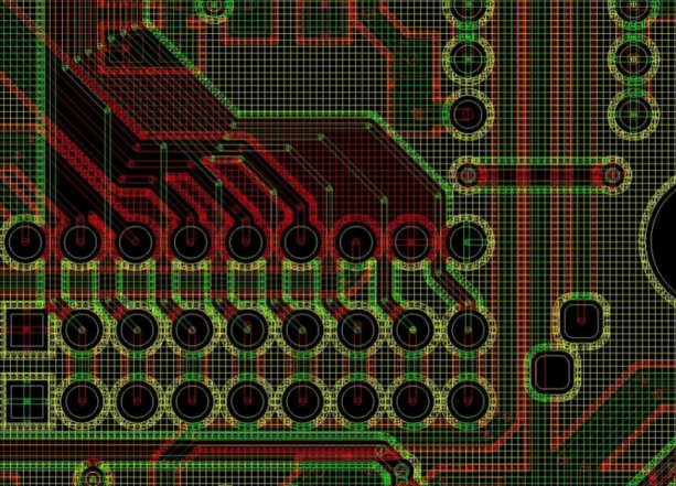
Figure 2-19: Gerber fill modes
Show Negative Objects: Select to toggle negative elements on and off.
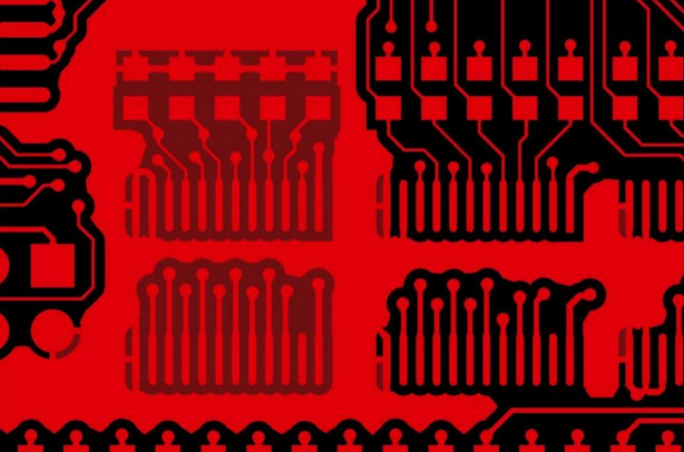
Figure 2-20: Show negative objects
Component Display Settings: Change component graphics and label display settings in the Comp layer. Centroid and BOM data must be loaded first to display Comp layers.
- a) Labels: Can choose between using Designators or Package name as labels if available
- b) Component Outlines: Display the component body and pin outlines from the chosen library or EDA package if available.
- c) Properties: Choose to display labels from nets, name, size, assembly type etc. and whether to show Polarity Markers.
- d) Text: Configure text properties including overflow behaviour and font size.
The settings can be saved for other projects by setting them as default.
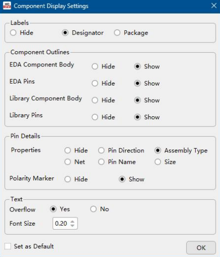
Figure 2-21: Component Display Settings dialog
Component List: Show the list of all components in the design with designators, part numbers, package, specifications etc. Click a part to highlight all instances of the component on the board, or click a designator to highlight the individual part. The search box can be used to search for a specific component using designators, part numbers, specifications etc..
3D Viewer: Open the 3D Viewer showing a realistic view of the PCB board which can be rotated in 3D space.
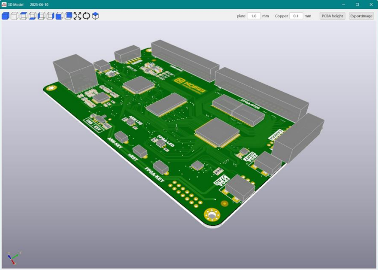
Figure 2-22: 3D Viewer of PCB and components
CAM/Real View Mode: Change between CAM (PCB) and Realistic view rendering modes.
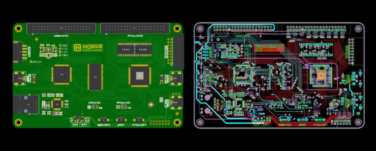
Figure 2-23: Realistic and CAM rendering modes
2.2.4. Operations menu functions
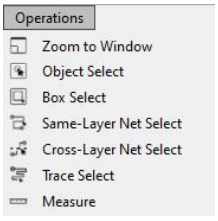
Figure 2-24: Operations Menu
Component List: Show the list of all components in the design with designators, part numbers, package, specifications etc. Click a part to highlight all instances of the component on the board, or click a designator to highlight the individual part. The search box can be used to search for a specific component using designators, part numbers, specifications etc.
Zoom to Window: Use the mouse to draw a window around the area to zoom into.
Object Select: Select an individual element by clicking them.
Box Select: Select a group of elements by drawing a box around them.
Same-Layer Net Select: Click a circuit element in the working layer to highlight the element and connected elements in the current layer.
Cross-Layer Net Select: Click a circuit element in the working layer to highlight the element and connected elements. Open multiple circuit layers in the Layer Manager to highlight connected circuits in other layers.
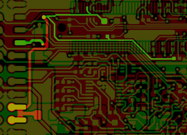
Figure 2-25: Cross layer net trace selection
Trace Select: Click a trace to highlight connected traces excluding pads.
Measure: Ruler tool for measuring various distances such as point-to-point distances, net, outline, centrepoint spacing and annular rings width. The measure dialog can be kept open while measuring lengths.
Figure 2-26: Measure options
▪ Point-to-Point:
Figure 2-27: Point-to-point length measurement
▪ Edge-to-Edge:
Figure 2-28: Edge-to-edge length measurement
▪ Net-to-Net:
Figure 2-29: Net-to-Net length measurement
▪ Annular Ring:
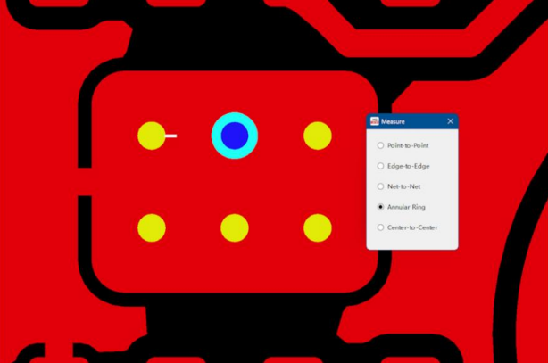
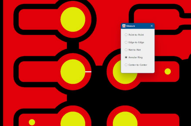
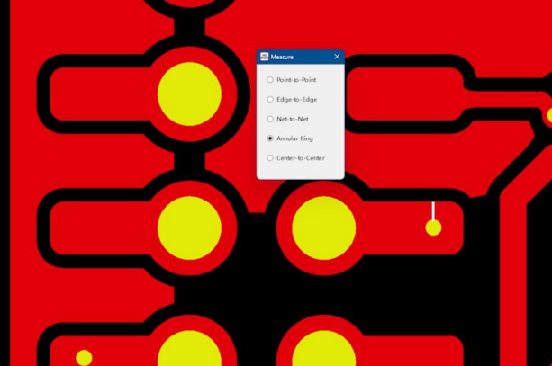
Figure 2-30: Annular ring length measurement
▪ Center-to-Center:
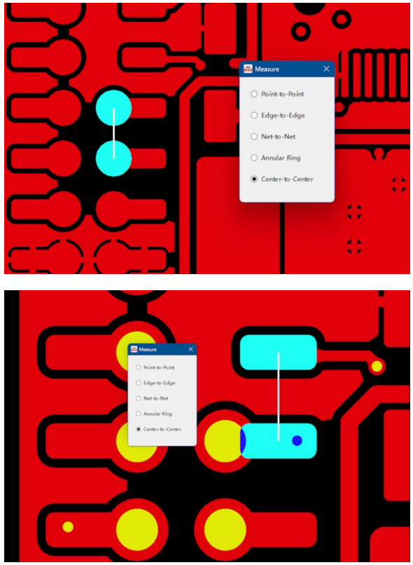
Figure 2-31: Center-to-Center length measurements
2.2.5. Tools menu functions
Further details on how to use the tools can be found in Chapter 2.
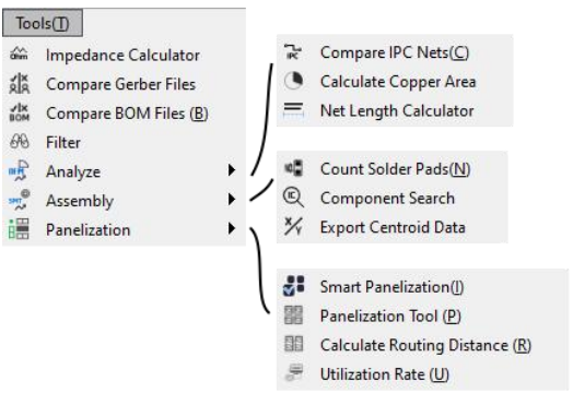
Figure 2-32: Tools Menu
Component List: Show the list of all components in the design with designators, part numbers, package, specifications, etc. Click a part to highlight all instances of the component on the board, or click a designator to highlight the individual part. The search box can be used to search for a specific component using designators, part numbers, specifications etc..
Impedance Calculator: Opens the Impedance Calculator tool for calculating the characteristic impedance of traces using real stack-up information.
Compare Gerber Files: Compare two sets of Gerber files and find differences between versions quickly.
Compare BOM Files: Find inconsistencies and changes in multiple BOM files quickly.
Filter: Search and filter elements such as parts by designator, package, value, or nets.
Analyze:
- a) Compare IPC Nets: Check for circuit shorts/breaks in the current design using IPC netlist files.
- b) Calculate Copper Area: Calculate the percentage area of the board covered in copper elements.
- c) Net Length Calculator: Calculate the length of multiple nets. Click [Select Net] then click a net in a circuit layer to add it to the list. Multiple nets can be added this way. Then click [Calculate] to retrieve the length and aperture size.
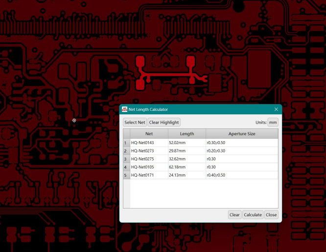
Figure 2-33: Net Length Calculator interface
Assembly:
- a) Count Solder Pads: Count the number of surface mount (SMD) and through-hole (THD) solder pads on the design to anticipate assembly costs.
- b) Component Search: Quickly locate a component on the board using centroid data. Centroid data must be uploaded to use this function.
- c) Export Centroid Data: Export the centroid/pick and place file for the current project including edits made in HQDFM. Valid centroid data must be uploaded to use this function.
Panelization:
- a) Smart Panelization: Provides various panel layouts based on different panel sizes.
- b) Panelization Tool: Customize panel design with more options including options for tooling rails, gaps, tabs and stamp holes for more complex panelization requirements.
- c) Calculate Routing Distance: Calculate routing lengths and visualize routing paths with different tool sizes to anticipate additional manufacturing costs.
- d) Utilization Rate: Calculate the utilization rate on standard production panels for optimal efficiency.
2.2.6. Board Settings menu functions
Board Settings: Configure board parameters for quoting and ordering purposes such as quantity, boardthickness, color, via type etc.
2.2.7. Settings menu functions
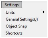
Figure 2-34: Settings menu
Units: Change the units for lengths from mils to mm or vice versa.
General Settings: Change basic settings, preferences and startup options including Analysis mode, export paths, language etc.
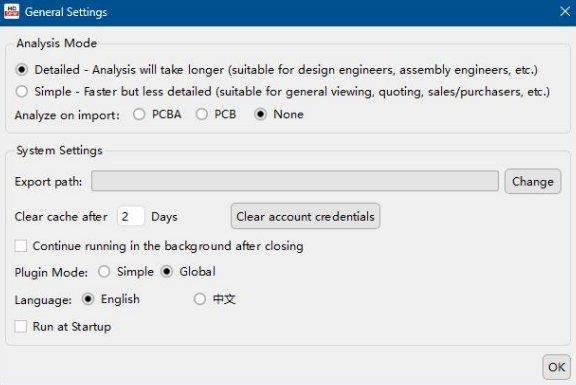
Figure 2-35: General Settings window
Object Snap: Change detailed object snap settings for more precise measurements. Snap settings only apply to the working layer or selected layers.
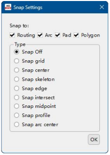
Figure 2-36: Snap settings window
- a) Snap center: Snap to the center of pads, drill hits, polygons or the center of end and start points used to create traces/line objects. Use the snap to skeleton setting to snap to the middle of traces/lineobjects.
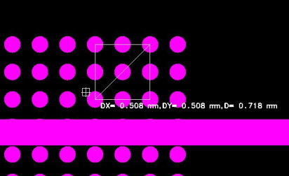
Figure 2-37: Snap to center settings used to measure the pitch of a BGA footprint
- b) Snap skeleton: Snap to the skeleton i.e. the center line used to draw traces.
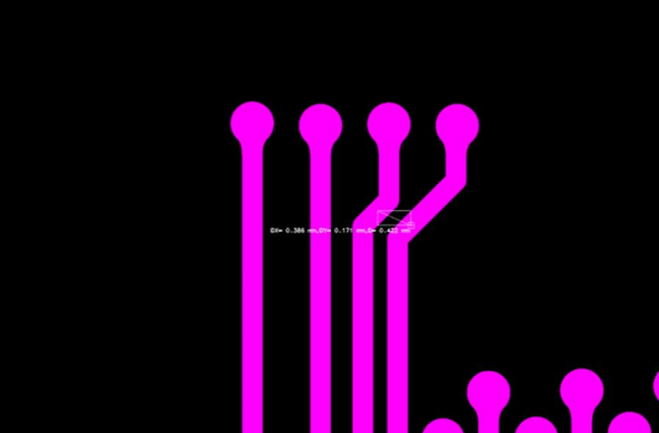
Figure 2-38: Snap skeleton settings used to measure the center-to-center distance between traces
Figure 2-39: Skeleton fill mode used to see the center lines of traces
- c) Snap edge: Snap to edges
- d) Snap intersect: Snap to intersections
- e) Snap midpoint: Snap to the midpoint of pads, drill hits, traces, etc.
- f) Snap profile: Snap to the profile
- g) Snap arc center: Clicking/hovering over an arc will snap to the origin of the circle used to createthearc.
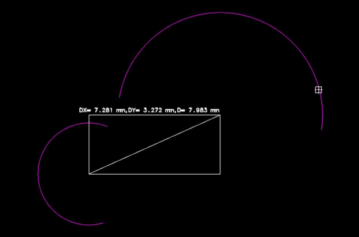
Figure 2-40: Snap arc center settings to snap to the center of the circle used to create the arc
Shortcuts: Set and customize keyboard shortcuts for various functions.
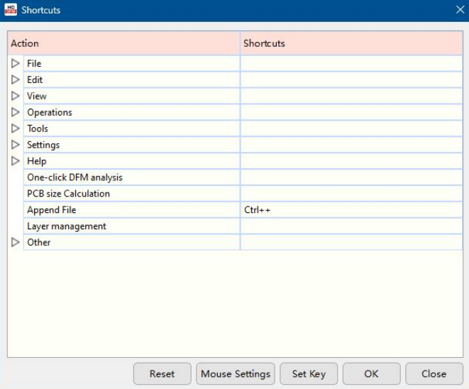
Figure 2-41: Shortcut settings window
2.2.8. Help menu functions
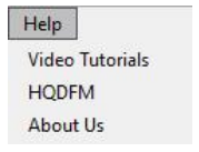
Figure 2-42: Help options
2.2.9. Online Support and Tutorials menu functions
Online Support: Shows the various contact methods to get in touch with NextPCB if you need any assistance with HQDFM or ordering.
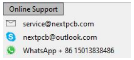
Figure 2-44: Online support contact methods
Tutorials menu functions: HQDFM User Manual opens the HQDFM User Manual web page.
Figure 2-45: Tutorials options
2.2.10. Rule Management
Customize DFM analysis thresholds for custom requirements (advanced). Custom rules can be exported and shared.
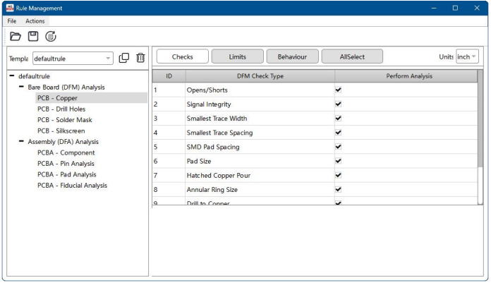
Figure 2-46: Rule Management window
Under the File menu, the custom rule settings can be imported or exported, under the actions menu, the rules can be reset to default settings.
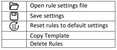
The rules are organized in a menu tree on the left. Click a sub-category to view and modify the analysis items on the right.
Figure 2-47: Rule Management categories
DFM Checks can be turned on and off by opening the Checks tab and checking the boxes on the right. Open the Limits tab to change the analysis range.
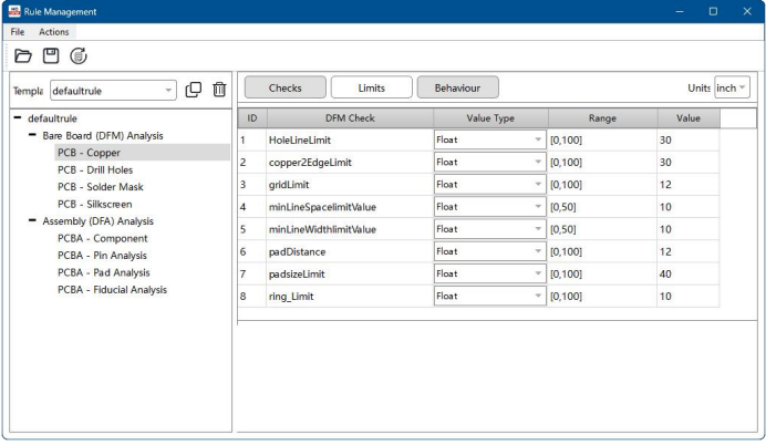
Figure 2-48: Analysis Limits settings
Click the Behaviour tab to modify the report warning thresholds and choose whether specific warnings are reported. For example, if the thresholds for minimum trace width are set as 3, 5, 6 mil:
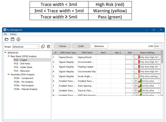
Figure 2-49: Report behaviour

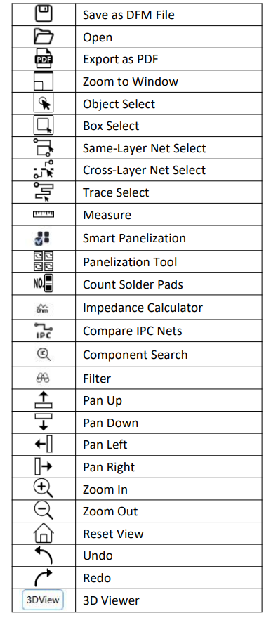
Figure 2-50: The HQDFM toolbar
2.3.1. Toolbar functions
2.3.2. Left Side Panel
1. DFM Analysis: Perform one-click Design for Manufacture (DFM) analysis for the plain circuit board design based on Gerber files or ODB++ files.
2. PCBA Analysis: Upload and configure centroid and BOM files for PCB assembly (PCBA) Design for Assembly (DFA) analysis including footprint and BOM checking.

Figure 2-51: DFM and DFA one-click analysis
3. CAM View/Real View: Switch between the CAM view to view individual Gerber layers and a realistic view of the manufactured PCB.
4. Create Profile: Manually calculate the board dimensions when HQDFM fails to recognize the board outline correctly. Select the outline elements using the box tool and click Create Profile. If no objects are selected, the entire working layer will be used for outline creation. In the new window, select an algorithm and the generated outline will be shown in white along with the calculated board dimensions.
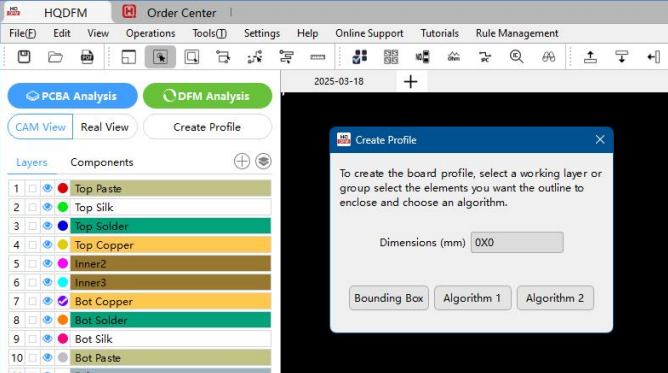
Figure 2-52: Create Profile dialog
2.4.1. Board Definition
A double-sided board typically has copper, solder mask and silkscreen layers for both top and bottom sides. HQDFM defines a single-layer board as having a single copper layer without plated through-holes and may have solder mask and silkscreen on one or both sides.
2.4.2. Required layers and Layer Assignment
HQDFM will try to match uploaded files with defined layers in the table below based on the file name and file extension. If it fails to assign the layer, the layer will appear on the bottom of the list labeled with the full file name.
If multiple layers are matched for the same layer e.g. two top solder mask layers or multiple drill files, the names of subsequent layers have label appended at the end. Detected blind/buried vias files will be labeled with the numbers of the connected layers accordingly (e.g. 1-5 top layer to the 5th copper layer).
| Full Name |
HQDFM Name |
Protel Extension |
Requirement |
Notes |
| Top component layer |
Top Comp |
-- |
|
Generated by HQDFM when Centroid and BOM data are uploaded. |
| Top paste layer |
Top Paste |
GTP |
Optional |
Paste layers are used to make stencils, these are not necessary for DFM analysis. |
| Top silkscreen (overlay) Layer |
Top Silk |
GTO |
Optional* |
Some designs do not require silkscreen on one or both sides. Without silkscreen data, silkscreen related problems will not be analyzed. |
| Top solder mask layer |
Top Solder |
GTS |
Required |
|
| Top copper layer |
Top Copper |
GTL |
Required |
|
| Inner copper layer (copper layer 2) |
Inner2 |
GL2 |
Required for multilayer boards |
HQDFM adopts the naming convention where the top copper layer is referred to as copper layer 1, therefore the adjacent copper layer is copper layer 2 and so on. |
| Inner copper layer (copper layer #) |
Inner# |
GL# |
Required for multilayer boards |
|
| Bottom copper layer |
Bot Copper |
GBL |
Required |
|
| Bottom solder mask layer |
Bot Solder |
GBS |
Required |
|
| Bottom silkscreen (overlay) layer |
Bot Silk |
GBO |
Optional* |
See top silkscreen layer notes. |
| Bottom paste layer |
Bot Paste |
GBP |
Optional |
See top paste layer notes. |
| Bottom component layer |
Bot Comp |
-- |
|
See top component layer notes. |
| Drill layer |
Drl |
DRL |
Required |
HQDFM uses the NC drill file in Excellon format for DFM analysis, not the drill drawing or drill guide/map. Multiple drill files can be uploaded for plated and non- plated holes etc. |
| Outline/mechanical layer |
Outline |
GKO/GML |
Required* |
Some designs include the board profile in other layers e.g. copper/silkscreen. This is not recommended as it can be misinterpreted. HQDFM will try to identify the primary mechanical layer if multiple mechanical layers are uploaded though it is recommended to include all profile elements in one mechanical layer. |
| Drill drawing |
Drl Draw |
|
Optional |
Not used in DFM/DFA analysis. |
| Drill guide/map |
Drl Guide |
|
Optional |
Not used in DFM/DFA analysis. |
| Milling layer |
Slot |
|
Optional |
Not used in DFM/DFA analysis. |
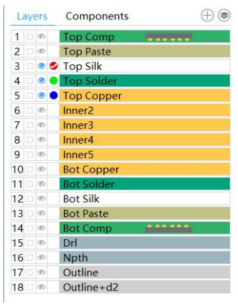
Figure 2-53: Meaning of icons and colors in the layer navigation panel
1. Show layer: Single-click a layer to toggle the layer visibility on and off in the workspace. The eye icon with a slash indicates the layer is hidden. The color of the circle represents the color of the layer in the workspace.
2. Show only one layer: Double-click a layer to open the layer and close all other layers. This layer is set as the working layer by default.
3. Set working layer: Click the colored circle of a layer to set it as the working layer.
4. Sync layers: Click the  checkbox to toggle selection. Checked layers will also be affected by actions in the workspace as if they were the working layer.
5. Show filename: Hover over the layer name to show the original filename.
6. Append layer: After importing Gerber files, click the plus sign icon to import more files to the current list of layers. This can useful for comparing files before and after modifications. Layers with the same name will have “+n” appended to the file name.
7. Open Layer Manager: Click the layer icon to open the Layer Manager window and change the layer properties including layer name, type, form and polarity. Drag the layers in the left list to rearrange the order.
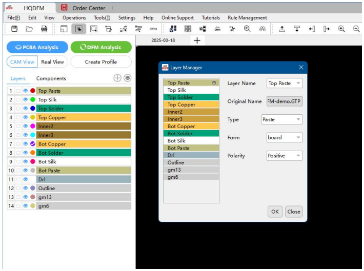
Figure 2-54: Layer Manager
2.5.2. Layer Navigation Panel Context Menu
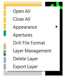
Figure 2-55: Layer navigation panel context menu
1. Open All: Open all layers in the workspace
2. Close All: Hide all layer in the workspace
3. Appearance:
- ▪ Set Color: Change the color of the layer as it appears in the workspace CAM view.
- ▪ Show Traces: Toggle show line objects such as traces.
- ▪ Show Pads: Toggle show flash objects such as pads and solder mask openings.
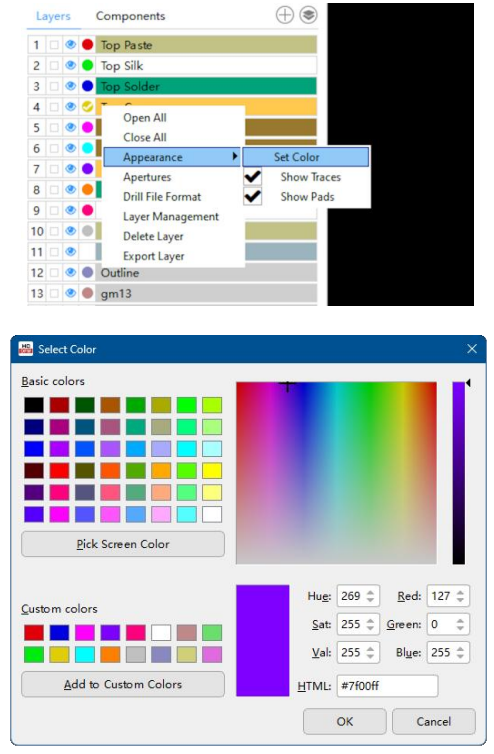
Figure 2-56: Layer color settings
4. Apertures: View the Aperture Table (Dcode) for the selected layer including size, polarity, quantity and highlight apertures in the selected layer.
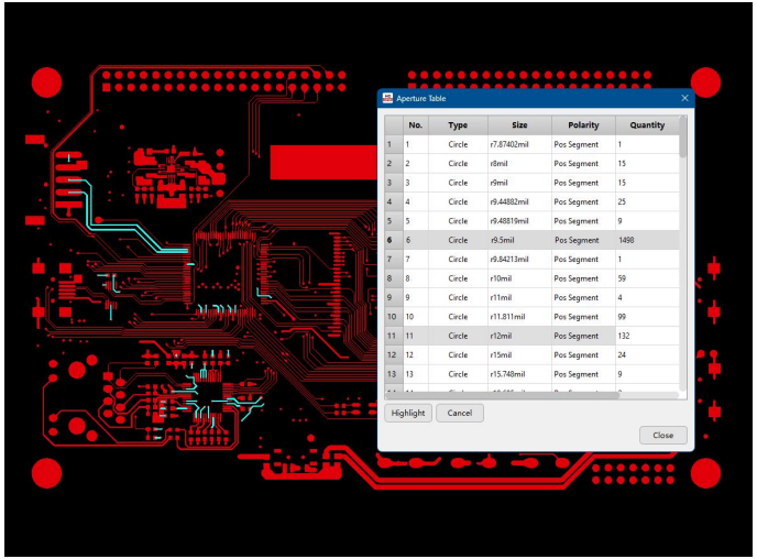
Figure 2-57: Aperture Table window
5. Drill File Format: View or change the import units for Excellon format drill files. Useful if HQDFM fails to detect the correct units or for extracting the units for other software and equipment.
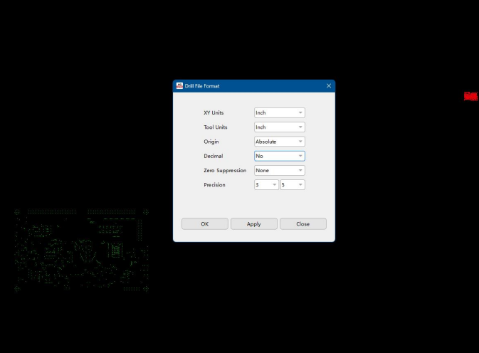
Figure 2-58: Drill file import units
6. Export Layer: Export the current layer including any modifications as a Gerber RS-274X file.
2.6.1. Who are NextPCB?
NextPCB provides PCB manufacture and assembly services with a focus on reliability without breaking the bank. With 5 factories in China and over a decade of quick turnaround electronics manufacture from prototype to mass production, NextPCB serves over 160 countries around the world with dependable electronics hardware paired with exceptional service.
Developed by NextPCB, HQDFM was developed utilizing in-house factory-floor expertise and industry insights to help designers, purchasers, contract manufacturers visualize and verify PCB designs. With HQDFM, NextPCB hopes to help both sides simplify and streamline the design to manufacture workflow.
Bare printed circuit boards of your design from NextPCB can be ordered directly from within HQDFM. The cost estimate and production time for 5 boards is displayed on the bottom right hand corner of the main window. The quantity and other board features can be edited using the [Board Settings] menu.
Please note that the board settings only include the most common customization options however, there are many more options on the NextPCB website.
As of the latest version (HQDFM International 4.6), only bare PCBs without components or assembly can be ordered within HQDFM. For turnkey assembly, please visit www.nextpcb.com for online quotations and more.
2.6.2. Board Settings
The number of boards, surface finish, board thickness, copper thickness, solder mask color can be changed from the board settings window to see how different options affect production cost and time.
Layer count and dimensions are extracted from HQDFM and cannot be changed from here. If these are incorrect, please close the window and re-calculate the board profile or check that the all copper layers have been correctly identified.
Click [Apply] to see the updated price and production time. Please note these are estimates based on the extracted parameters and board settings. There are circumstances or features that HQDFM is unable to extract which may affect cost.
Settings stored in JSON format can be exported for backup, transfer, or sharing purposes.
2.6.3. Steps: How to order PCBs
1. Upload your design's production files (Gerber and drill or ODB++) in HQDFM. Learn how to create Gerber files
2. Change boards settings if necessary
3. Any applicable discounts will be applied. Make sure you are logged in to apply discounts applicable to your account.
2.6.4. PCB cost and production time estimate calculation
HQDFM will calculate the production cost and time of bare PCB fabrication from NextPCB once production files have been loaded. This cost estimate is based on the layer count, PCB dimensions and the configuration set in the Board Settings menu.
A more detailed cost estimate can be obtained by performing DFA Analysis. This will extract other details such as trace width and spacing, smallest drill hole size, smallest pad size, blind/buried vias, test point count and milling density, all of which can affect production cost and time.
After performing DFA analysis, check for reported DFM errors, particularly for any of the items mentioned above.
If the cost is unusually high, compare the cost before and after performing DFM analysis. If the cost increases, there may be features in the design influencing the cost. Check DFM errors such as trace width and spacing, which may impact cost.
HQDFM can perform two types of analysis, PCB Design for Manufacture (DFM) and PCBA Design for Assembly(DFA):
1. PCB Design for Manufacture: Analyzes PCB production files to highlight errors and evaluate the manufacturability of the design using modern PCB fabrication methods.
2. PCBA Design of Assembly: Analyzes Centroid, BOM and footprint data against the PCB production files to highlight errors and evaluate ease of assembly with modern PCB assembly methods.
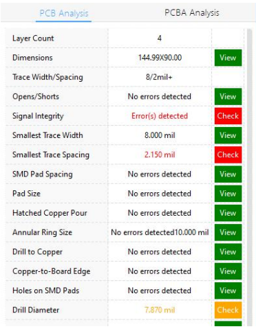
Figure 3-1: DFM Results Panel for PCB and PCBA
HQDFM's algorithms analyze manufacturing data (Gerber files, ODB++ files, Centroid data, and BOM) for errors affecting production, assembly, reliability, and cost, based on industry-wide PCB manufacturing and assembly capabilities.
As different manufacturers have different capabilities, HQDFM provides a three-tier error reporting system, where the highest tier includes critical errors that only the most advanced manufacturers can handle.
The three error severity levels are as follows:
- 1. High Risk (Red)
A red alert indicates a critical issue that needs immediate attention and likely design changes. These problems stem from design features that may surpass manufacturing capabilities, result in high defect rates, introduce significant complexity, or adversely affect the product's long-term reliability and performance.
Action: Such designs are likely to be rejected by manufacturers or result in non-functioning or defective boards. Action is strongly recommended.
- 2. Warning (Yellow)
Yellow alerts indicate issues that require review. They may result in additional costs, a higher defect rate, lower reliability or assembly complications.
Action: These designs may be rejected by less advanced manufacturers, incur additional expenses, extend lead times, or have hidden impacts on long-term reliability. The severity of these issues varies and should be assessed based on the specific design requirements. Review and evaluation are recommended.
- 3. Pass (Green)
No errors were detected and the design is within the manufacturability limits of most PCB fabricators and assembly houses.
3.3.1. Six Types of Errors Detected
There are generally 6 types of errors that HQDFM will detect and report:
a) Design errors impacting functionality: Issues such as shorts or open circuits that can compromise the board's performance. Errors affecting reliability or performance: Designs that can be manufactured but push the limits of acceptable tolerances.
- ▪ Example 1: Insufficient copper spacing increases the risk of shorts over time due to Conductive Anodic Filamentation (CAF), where salts grow between copper elements along the PCB substrate, potentially bridging gaps.
- ▪ Example 2: Inadequate copper-to-edge spacing can expose copper during board routing, making it prone to shorts, corrosion, and delamination over time.
b) Designs exceeding manufacturing capabilities: Features that go beyond the technical limits of most production facilities.
c) Complex designs with high risks: Features that introduce significant manufacturing challenges, potentially leading to high failure rates, additional costs, or extended lead times.
d) Manufacturing Compatibility: Elements that may not be viable for mass production, specific assembly types, or general repair. For instance, wave soldering requires more design considerations than reflow soldering, and the absence of solder mask dams can complicate manual repairs even if they don't affect reflow assembly.
e) Gerber generation errors: Issues arising during the translation of design data into Gerber files. Poor implementation or incorrect export settings can introduce errors not detected by the EDA tool's DRC(Design Rule Check), potentially leading to critical failures.
3.3.2. DFM/DFA Analysis Forewarning:
Due to the complexity and differences of manufacturing practices and the limited information available, the accuracy of the reported errors will vary on a case-by-case basis. As always, HQDFM is best usedalongside expert review and manufacturer feedback. The following notes should be observed when using HQDFM analysis capabilities:
▪ Data Availability: HQDFM performs analysis on standardized production data commonly requested by manufacturers (Gerber/ODB++ 2D graphical data, component placement data and footprint information if available).
▪ Other Information: HQDFM does not know or make use of other information such as the intended assembly method (reflow/wave soldering), production volume (prototype/mass production), industry or certifications, functionality, design tools or any information included in other production documentation including PCB parameters such as solder mask color or PCB material. As a result, HQDFM makes conservative assumptions and may appear overly cautious when reporting errors, although we try to limit this as much as possible. It is the user's responsibility to check and verify the accuracy of the reported errors based on their knowledge product's requirements and intended production methods. While HQDFM attempts to provide guidance in the formof tiered warning levels, the final decision rests with the user.
▪ Non-standard Data: Due to the limitations of 2D binary data formats and inconsistent EDA software implementations, non-standard Gerber, Excellon and ODB++ data may cause HQDFM to misinterpret certain features and provide false negatives or positives. In most cases, designer have limited control over these reported errors but many can be safely ignored. There is also a feature to ignore certain checks in HQDFM if needed.
▪ HQDFM does not tell you if your boards are or are not manufacturable: HQDFM is intended to complement DRC (Design Rule) checks and manual verification to reduce errors and optimize reliability and efficiency. Not all errors are related to manufacturability and so if errors are reported, this does not necessarily mean the boards cannot be manufactured or will encounter problems. Likewise, the absence of errors does not necessarily mean your boards can be manufactured.
Manufacturer capabilities and preferences vary and while new algorithms are being developed or improved all the time, HQDFM is not able to detect all possible manufacturing problems.
3.4.1. Perform DFA Analysis:
1. Upload production data. A set of Gerber and drill files or ODB++ files must be uploaded in order for the algorithms to perform correctly. See table # for the required Gerber and drill files.
2. Click the green [DFA Analysis] button on the left panel and wait for analysis to finish. Larger, more complexfiles will take longer to process.

Figure 3-2: PCBA Analysis and DFM Analysis buttons
3. The results of DFM and DFA review will be shown on right side of the workspace. Clicking the [View] or [Check] button will open the corresponding pop-up window and/or change the workspace view.
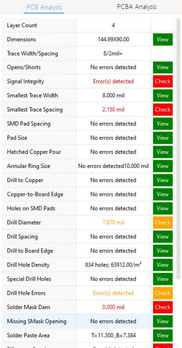
Figure 3-3: PCB DFM Analysis items
4. It is recommended that all high risk and warning errors reported by HQDFM are checked by clicking [Check]and viewing the issues in the DFM/DFA navigation window.
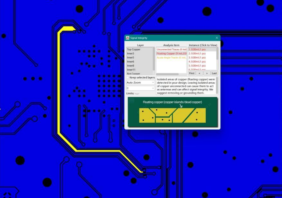
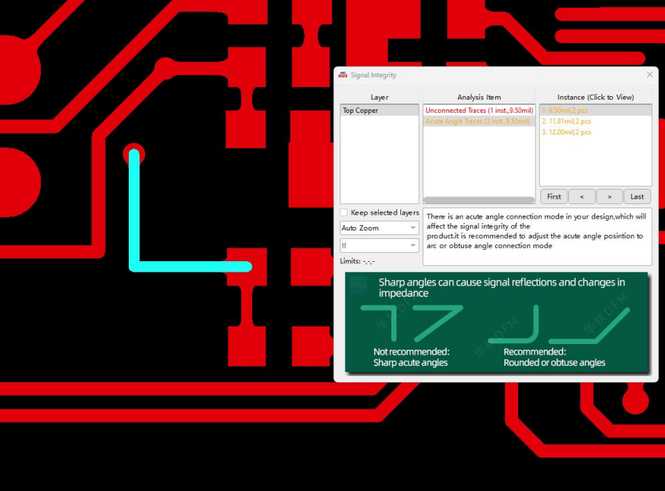
3.4.2. DFM/DFA Navigation Window
The DFM/DFA navigation window shows the details of any identified problems and can be used to pan to the location of the occurrence in the workspace.
a) Layer: Layers/sides where issues were found will be shown here. Click an individual layer to show the issues in that layer/side only, e.g. top or bottom side.
b) Analysis Item: Sub-items of the main analysis item will be shown here. Click a sub-item to show the occurrences on the right.
c) Occurrence: All occurrences of the sub-item will be listed here. Click a field or use the navigation buttons to zoom in and/or pan to the occurrence according to the navigation settings. The offending elements will be highlighted and lengths will be indicated by a white line.
d) Navigation settings: Select how the workspace view changes when an occurrence is selected.
- ▪ Auto Zoom (default): Pan and zoom into the location of the occurrence.
- ▪ Pan Only: Only pan to the location of the occurrence. The previous zoom level is preserved.
- ▪ Pop Up: Displays a pop-up viewer over the workspace zoomed in on the location of the occurrence.
e) Error Display settings: Choose whether to show High Risk errors (!!), Warnings or show all possible analysis items in the current category (Show All).
f) Limits: The current analysis item's threshold limits (Red - Yellow - Green)
g) Description: Text description detailing the error and any extracted values.
h) Graphic: A supporting graphic for the analysis item.
3.5.1. Layer Count
Display of the number of copper layers in the design. HQDFM will infer the layer count by counting the number of copper layers imported into the workspace. If this is incorrect, HQDFM may have failed to assign a copper layer. Manually assign unmatched layers and re-run DFM analysis.
3.5.2. Dimensions
Display of the board dimensions calculated from the imported design. This is calculated from the board profile. If this is incorrect or empty, the board outline may be missing or not located in a dedicated outline layer. Export the outline from the design tool or use the Create Profile tool to reconfigure the profile.
3.5.3. Trace Width/Spacing
Display of the smallest trace width/spacing in the design. This is calculated from all the copper layers uploaded in the design. Order forms often request the minimum trace width/spacing to provide a quotation and gauge the technical complexity of a design. The largest value displayed is 8mil (0.2mm) even if the smallest width/spacing is greater than this.
For details, refer to the individual Smallest Trace Width, Smallest Trace Width analysis items below.
3.5.4. Opens/Shorts
Clicking [View]/[Check] opens the Compare IPC Netlist tool. If the netlist file was already uploaded with the Gerber files, this check will run automatically.
3.5.5. Signal Integrity
Signal integrity problems are related to the circuitry. They are not necessarily related to manufacturing but may have a significant impact on functionality or performance.
3.5.6. Smallest Trace Width
The width of the narrowest copper trace in the design. Each PCB fabricator has a minimum capability typically stated on their website or design specifications. Designing traces narrower than this specified minimum can lead to an exceptionally high defect rate (e.g. broken or incomplete traces) or outright rejection of the design by the manufacturer.
Designing near a manufacturer's limits should also be avoided whenever possible, as it can lead to increased costs, added manufacturing complexity, and a higher-than-normal defect rate.
3.5.7. Smallest Trace Spacing
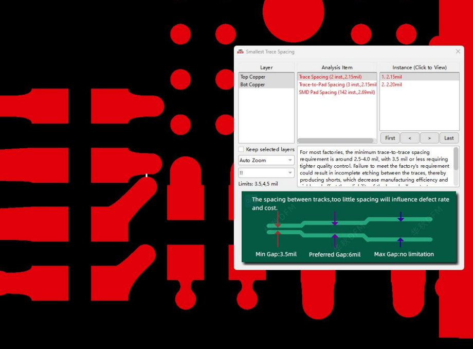
The smallest distance between two copper traces or other copper elements of different nets in the design. Like trace width, each PCB fabricator has a minimum capability typically stated on their website or design specifications. Traces closer than this specified minimum can lead to an exceptionally high defect rate(e.g. incomplete etching and short circuits) or outright rejection of the design by the manufacturer.
Designing near a manufacturer's limits should also be avoided whenever possible, as it can lead to increased costs, added manufacturing complexity, and a higher-than-normal defect rate.
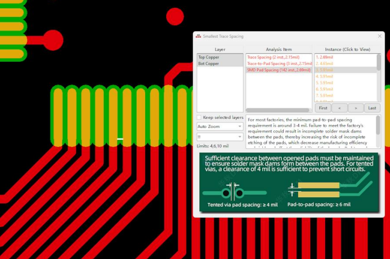
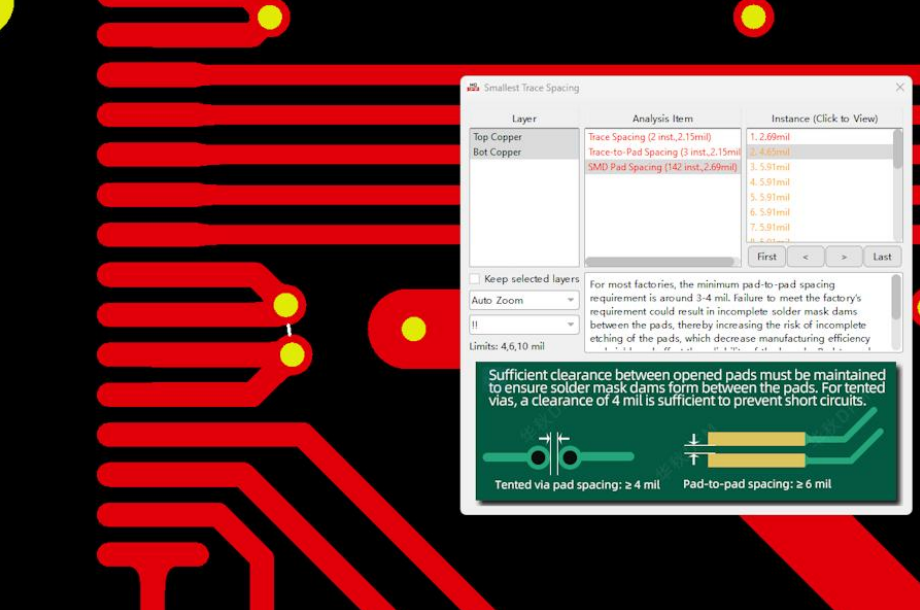
3.5.8. SMD Pad Spacing
The distance between open pads of surface mount parts.
3.5.9. Pad Size
The size of open pads on the design. If pads are too small, they become harder to etch accurately and may detach more easily. Additionally, pads that are undersized can pose challenges during testing, as they may be too small for testing probes to establish consistent and reliable electrical contact.
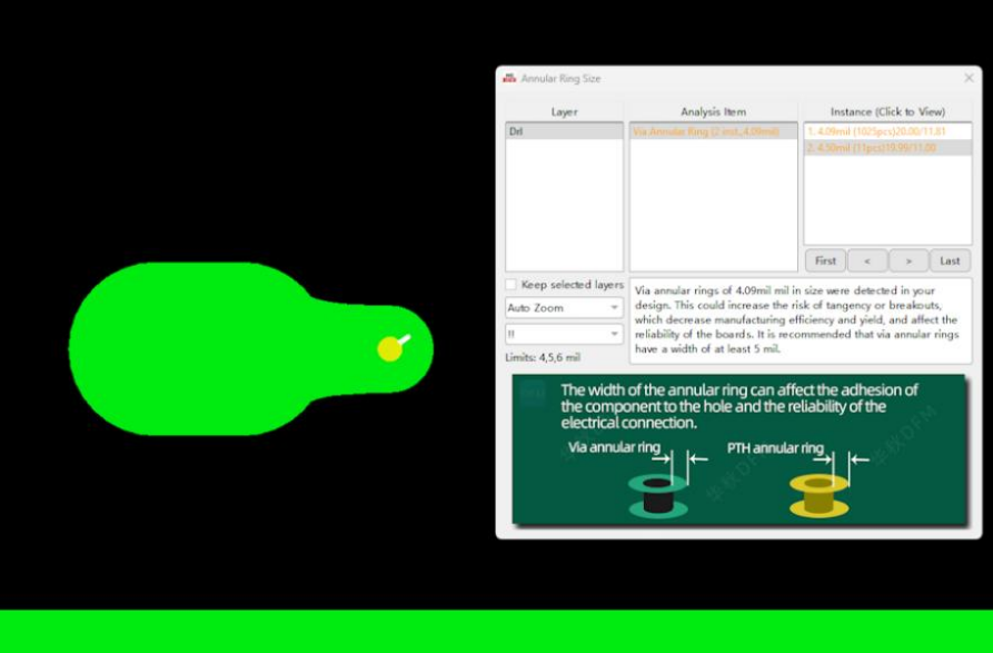
3.5.10. Annular Ring Size
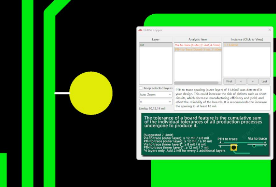
3.5.11. Drill to Copper
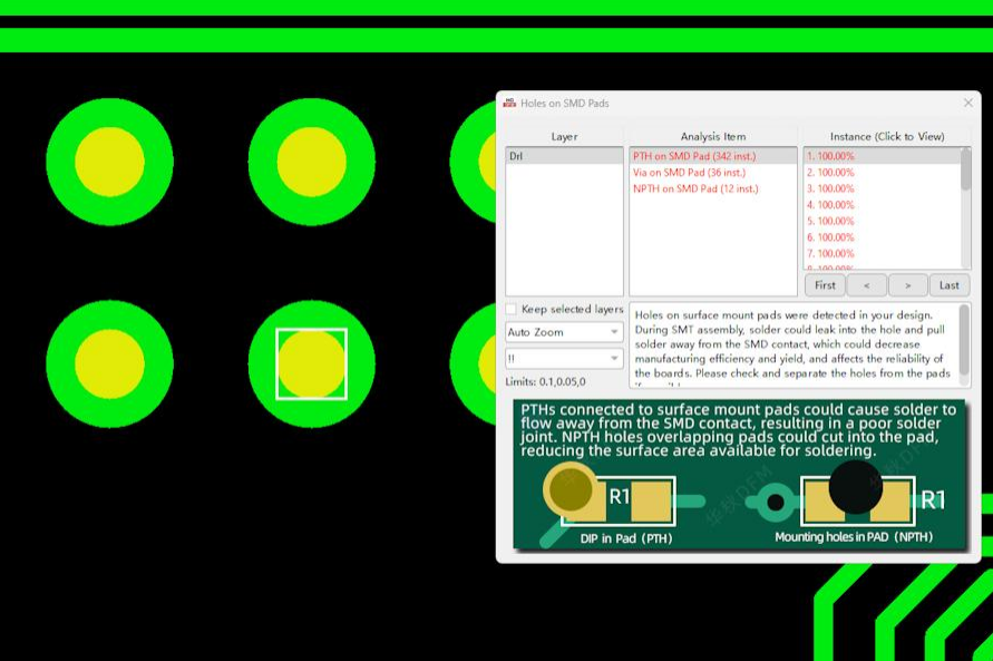
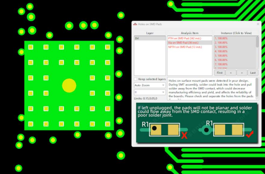
3.5.12. Holes on SMD Pads
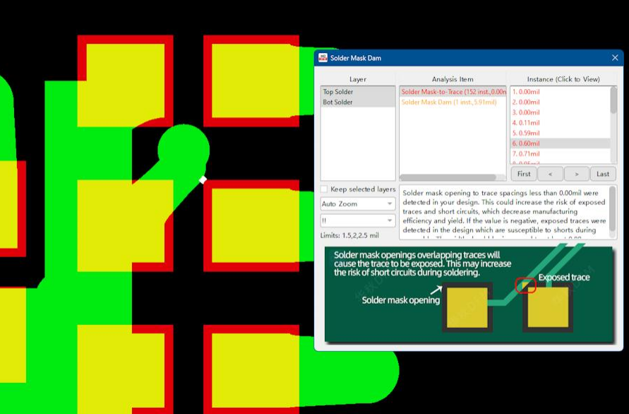
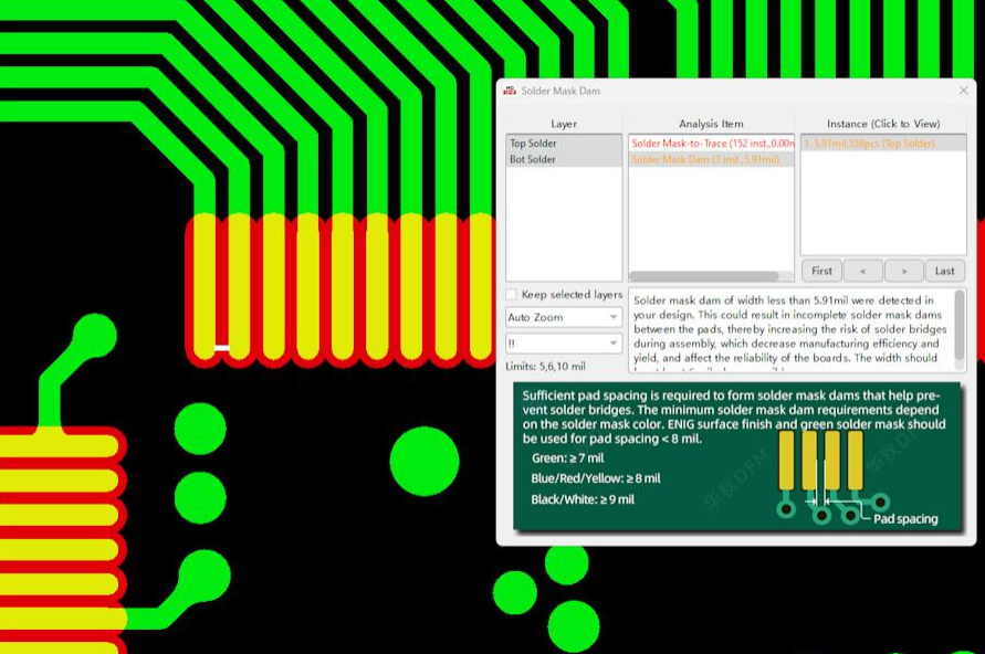
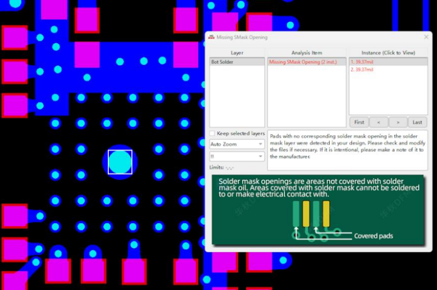
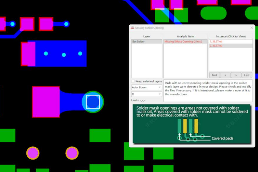
3.5.13. Missing Smask Opening
Explore NextPCB’s PCB Manufacturing Capabilities
DFA stands for Design for Assembly, and in the electronics hardware manufacturing industry, assembly typically refers to the stage of populating a bare circuit board with components. Like DFM for bare PCB boards, DFA provides design guidelines to optimize the assembly of a product in terms of yield, efficiency, reliability and cost.
In addition to PCB Design for Manufacturability, HQDFM also has advanced DFA capabilities and tools, giving design engineers a complete suite for optimizing the entire electronics manufacturing and assembly process from the outset.
Like DFA Analysis, HQDFM can perform over 600 detailed DFA checks in 12 categories based on IPC guidelines and NextPCB's own assembly experience. HQDFM also has a powerful footprint checker with over 5 million package libraries and counting, maintained by over 20 full-time engineers, and is also equipped with other tools such as the handy BOM checker and centroid file editor, helping engineers cut down on mundane administrative tasks and human errors.
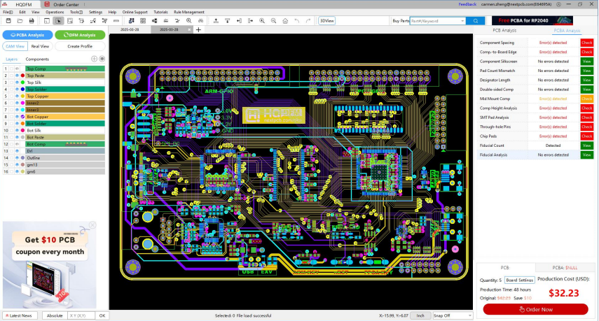
Figure 4-1: Main interface after PCBA DFA analysis
With the addition of DFA analysis capabilities, HQDFM is a complete suite for engineers to produce effective prototypes fit for market, accelerating and streamlining product development with minimal waste.
For DFA analysis, in addition to bare PCB production files, the Bill of Materials (BOM) and component centroid, also known as pick and place, data is also needed.
4.2.1. PCB Production Files (Gerber/Drill/ODB++)
PCB Production Files: Include PCB Gerber files in RS-274x or X2 format and PCB drill files in Excellon format. Direct KiCad (.kicad_pcb) upload is also supported.
Gerber Files/Drill files: As for DFM analysis, import Gerber and drill files by clicking New File and selecting all files or the archive file containing the files. You can also drag and drop the files from file explorer directly.
ODB++ files: Open ODB++ production files by dragging them into the workspace or clicking the "NewFile" button and selecting the file.
4.2.2. Bill of Materials (BOM):
The bill of materials or BOM file contains a list of all the components to be populated onto the PCB with their respective quantities and designators, or labels per individual board or panel.
Other information is often included such as package name, description, purchase link, value, alternative parts etc. and other PCB features may be included such as test points and fiducial marks which do not require procurement or soldering.
Like Gerber files, many EDA packages support internal editing of a BOM file which can then be exported, though the format, content and labels will vary across packages. A template can be downloaded from the wizard.
To perform DFA analysis and footprint checking, HQDFM requires the BOM file to include the following three pieces of information at the bare minimum:
a) Manufacturer's Part Number (MPN): This is the unique part number assigned by the manufacturer fora specific product. It should not be confused with the distributor's SKU number such as Digikey Part Number or LCSC Part #.
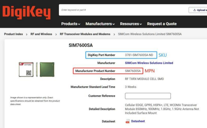
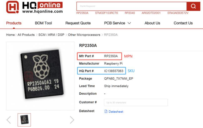
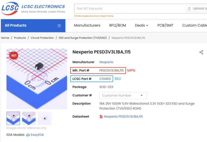
Figure 4-2: Screenshot showing the SKU and MPN values of a component on Digikey, HQOnline andLCSC
b) Designator: The designator is the unique identifier assigned to each component on a PCB (PrintedCircuit Board). It helps to identify and locate the specific components during assembly, testing, and troubleshooting.
- Resistors: R1, R2, R3..
- Capacitors: C1, C2, C3..
- Integrated Circuits (ICs): U1, U2, U3..
- Diodes: D1, D2, D3..
c) Quantity: This indicates the total number of pieces of a component needed for the board. Since a PCB BOM file typically corresponds to a single non-panelized board, the quantity should match the total number of designators listed for that part.
4.2.3. Centroid files:
Centroid files, also referred to as pick and place files or component placement files, are used by pick and place machines to accurately position and orientate surface mount parts on a PCB. The file typically includes a list of the X-Y coordinates, rotation angles and side (top/bottom) information for all surface-mount parts and may also list through-hole parts, test points and fiducials.
Centroid files are exported from the EDA software and may have customization options such as splitting the data into separate files for top and bottom sides, or include through-hole parts, which is preferred by some pcb manufacturers.
These files are typically exported in excel spreadsheet, text or csv file format. HQDFM accepts files in .xls, .xlsx, .csv and .txt file formats and at the bare minimum, the Designator, X-Y coordinates, rotation and side information is required. A template can be downloaded from the wizard for reference.
For DFA analysis, the centroid file should contain all parts on the board (top and bottom) in a single file along with through-hole parts if possible. Without location information for through-hole parts, HQDFM cannot perform DFA analysis on them.
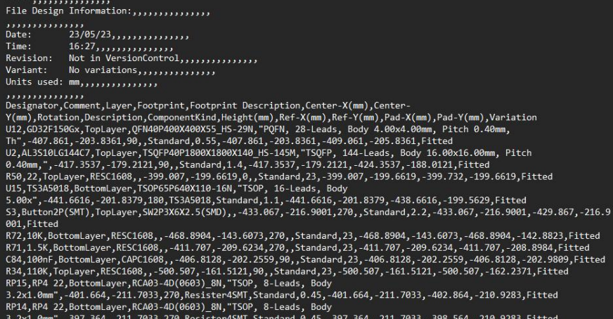
Figure 4-3: Sample centroid/pick and place file exported from an EDA tool
HQDFM uses the three above sets of files to determine the location and rotation of parts, which parts require assembly and their respective footprints on the PCB board. These are necessary to perform footprint checking, BOM checking and DFA analysis.
Steps:
1. First import the PCB design into the workspace by importing the Gerber/Drill files or ODB++ file.
2. Then click the blue [PCBA Analysis] button on the left panel to open the DFA Analysis wizard.
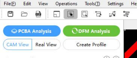
Figure 4-4: PCBA and PCB DFM Analysis buttons
The wizard is separated into 5 steps as indicated at the top of the window:
1. Centroid: Import and configure the centroid file. Learn How to Create a Centroid (Pick & Place) File Instantly
2. Import BOM: Import and configure the Bill of Materials file
3. Match Parts: Perform parts matching with HQ's package database and view detected errors.
4. Part Type: Modify part types property of matched parts for accurate DFA analysis
5. Direction: Set the direction of travel in assembly equipment
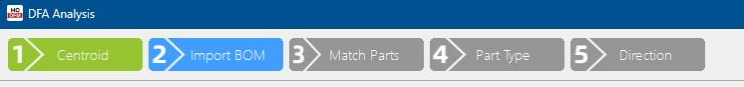
Figure 4-5: DFA Analysis steps
At any point, you may search for a specific part by entering it's designator in the search bar on the top right. File header and package matching settings can be changed by clicking the [Match Settings] button.
Figure 4-6: Search Component search bar and Match Settings options
For a basic DFA analysis, you can utilize the wizard to upload and set up the centroid and BOMfiles, and skip the other steps. The subsequent section will provide a detailed explanation of each part of the wizard and its functionality.
4.4.1. Centroid File Import and Configuration:
1. Load Centroid File: Import centroid files by clicking the [Load Centroid File] button and either browse for the file or drag and drop it directly into the window. Once imported successfully, the wizard will display a preview of the centroid data in a spreadsheet format. Quick Guide: How to Create a Centroid (Pick and Place) File Instantly
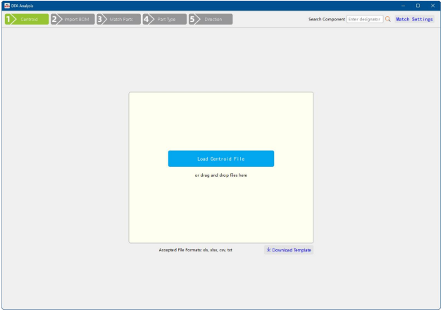
Figure 4-7: Load Centroid File stage
2. Assign headers: The headers in the centroid file must be correctly assigned for accurate analysis. HQDFM will try to identify the headers by matching them with keywords saved in the database. If they are incorrect, click the drop down box and select the correct fields.
Tip: If a field has already been used, it will not appear in other drop down boxes. Free it up by first changing the incorrect value to the default letter value.
3. Remove extra rows: Remove empty row entries that do not contain centroid information suchas extra header information that has not already been removed by HQDFM by clicking [Delete]. Rows and columns can be added or deleted by right-clicking the row number or column header and using the context menu.
You can also add rows and columns and edit the contents of the BOM file by double-clicking the cell.
a) The original file contents can be viewed by selecting the Original tab and you may start again or change files by clicking the [Re-upload] button and uploading files again.
b) Click [Next] button or the [Render Image] on the right to generate the component layer which is shown on the right preview windows for both top and bottom sides. The component layer consists of place- markers and basic part outlines if available, which is overlapped on top of the PCB pads in the preview windows. Use this to verify correct placement and orientation.
The preview allows for zooming in and out, scrolling and panning just as in the main workspace, and clicking a row in the spreadsheet will zoom into the corresponding location in the workspace. If the placement is correct, click [Next] again.
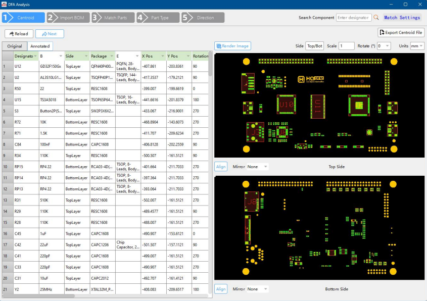
Figure 4-8: Centroid file editing interface
c) If the top and bottom values are not identified correctly, the matching keywords can be viewed and modified by clicking the Side box. To add new keywords, type them in the relevant field and separate them with a comma.
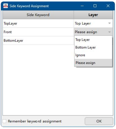
Figure 4-9: Top/Bottom side keyword assignment window
4.4.2. Editing Centroid Files
The following centroid file editing features apply to the entire centroid file i.e. all values in the list are changed. For individual component changes, the values in the spreadsheet can be modified directly by double-clicking the cell. Click the Render Image button to update the preview windows.
▪ Scale: Changes the XY coordinates by a scale factor. The default value is 1. This is useful if the centroid and PCB production data have different scales.
▪ Rotation: Changes rotation angle by a fixed amount. This is useful if the PCB data was rotated for panelization for example, in which case the centroid data should also be rotated.
▪ Units: Converts the XY coordinate values into other units. Units in mm, inch and mils are supported.
▪ Align: Opens the Align tool to graphically align the component layer with the PCB pads, then converts the centroid file XY coordinates accordingly.
▪ Mirror: Reflects the component layer in the X or Y axes. To reflect in both axes, select one after the other.
The edited centroid file can be exported .xlsx format using the [Export Centroid File] button. Choose which columns to export with the [Add Column] and cross buttons and customize the sequence by dragging them to the desired position.
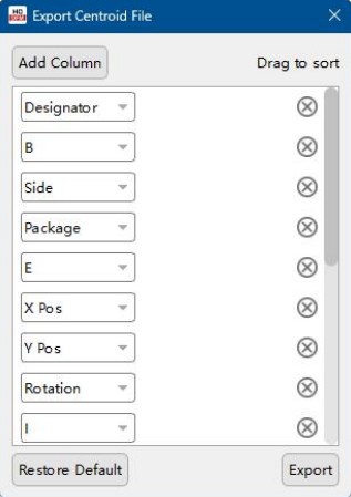
Figure 4-10: Export Centroid File interface
The exported Centroid file contains the contents of the Annotated File after post-processing and any adjustments made.
4.4.3. Align Tool
Use the align tool when the entire component layer is displaced by a fixed distance. Followthese steps to perform alignment:
1. Open the align tool by clicking [Align]
2. Click [Select Part] and click a part in the component layer, preferably a symmetrical part with few pads. The selected part will be highlighted and the designator will be shown next to the button.
3. Click [Select Pads] and click the pad or pads whose centre is the selected component's origin. E.g. the two pads of a chip resistor, or an IC's central thermal pad. Highlighted pads will be shown in blue. Multiple pads can be selected by holding the Ctrl key while clicking the pads. Check the Sync bottom layer box to move the bottom layer by the same distance if desired, then click Align.
Figure 4-11: Examples of simple components with good pad symmetry and selected pads suitable for defining the component origin.
4.5.1. Load BOM file
a). Similar to loading Centroid files, import BOM files by clicking the Load BOM File button and browsing for the file or dragging it into the window directly. Upon successful import, a preview of the BOM data in spreadsheet form will be shown in the wizard.
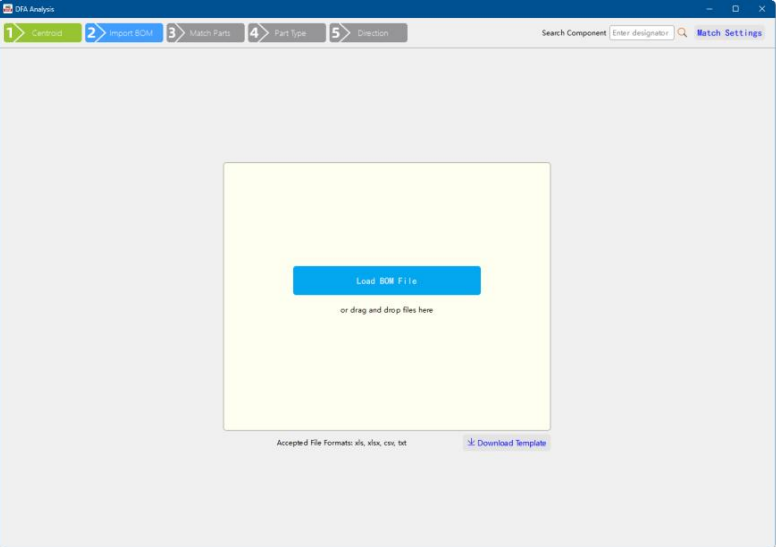
Figure 4-12: Load BOM File stage
b) Again, assign the headers manually if incorrectly matched by HQDFM by selecting them from the drop down box. The more information available to HQDFM the better the analysis results.
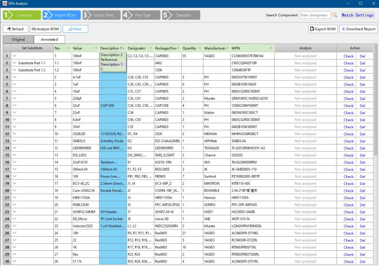
Figure 4-13: Edit BOM file and assign headers interface
c) Remove unnecessary rows using the Del (Delete) option in the Action column or by right clicking the row number.
d) View the original pre-processed BOM data by clicking the Original tab. If you make a mistake and need to start again or change files, click the Reload button.
e) Click the [Analyze BOM] to check the BOM for errors or [Next] to skip this step.
4.5.2. BOM Analysis
BOM analysis is an optional but highly recommended step to analyze the BOM file for inconsistencies and errors such as duplicate designators, inconsistent parameters and incorrect quantities.
1. Click the [BOM Analysis] to initiate BOM processing and HQDFM will compare the designators in BOM with the centroid file.
2. HQDFM will perform a quick analysis and the results will appear in the Analysis column to the right of the original data. Any detected errors will appear in a red box. Hover over the box to display the full details. Review these errors before moving onto the next step. A summary of the errors can also be exported by clicking the Download Report button.
3. Not in centroid file: the centroid file contains parts that are not in the BOM file. This could be due to accidental omission or purposely removed since it is not needed in this specific version. It could also be the result of only exporting surface mount components in the centroid file. HQDFM can perform analysis on through-hole parts as well so include these in the centroid data if possible.

Figure 4-14: Designator missing warning
4. Qty/Designators mismatch: HQDFM will count the number of designators and compare it with the value marked in the Quantity column. This error will appear if there is a discrepancy between the two. Either value can be modified directly by double-clicking the cell and typing in the new value. Then click the Check option in the Action column to repeat analysis on this row and remove the error message.

Figure 4-15: Quantity/designator mismatch warning
5. Repeated Designator: HQDFM will compare the designators across the entire BOM to find duplicates. Each designator should only correspond to a single part number and most of the time should only appear once in the BOM file. HQDFM will highlight any duplicates and indicate the row number where the duplicates appear.
In some cases, duplicates in a single row (same part) are acceptable. For example, for boards that are repeated in a panel, the repeated boards have the same designator markings, therefore the BOM may have many duplicates designators. These can be safely ignored.
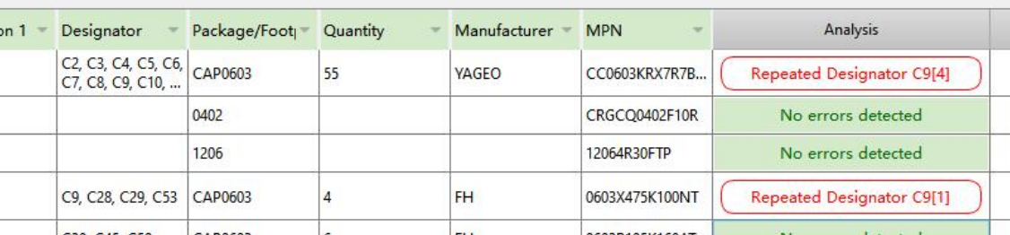
Figure 4-16: Repeated designator warning
6. Package mismatch: HQDFM will capture keywords in the package field and compare them with the description field to find discrepancies. For example, if the part has a PCB footprint of 0402 but the chosen part has a size of 1210, this will be highlighted and designers should change the part or footprint.
Due to different unit systems being used, HQDFM may highlight a mismatch incorrectly. For example, the LED in row 12 has the imperial size of 1210 but the package is written according to the metric size (3528). In such cases, the errors can be safely ignored and changing the package name to 1210 will clear this error.

Figure 4-17: Footprint error warning
7. Once all errors have been reviewed and rectified, click Next to proceed to the next step.
8. If modifications were made, the BOM file can be exported using the [Export BOM] option. Select columns to include and drag them to change the order.
4.5.3. Substitute Components
HQDFM supports the inclusion of substitute components in the BOM that can also take part in DFA analysis. To do this, they must have their own row with footprint information, description and part number etc.
1. In the BOM, add a new row under the original part. The index number should be the original index number followed by a period and a number from 1 to 9 with .1 being the first substitute part e.g. 1.1, 1.2, 1.3, 1.4, 1.5 etc. 1.2 would be the second substitute part for the primary part in row 1.
For substitute parts, only the MPN is required. Other information such as designators and quantity will be taken from the primary part.
2. Upon importing into HQDFM, the software will recognize these as substitute parts and label them accordingly in the Substitute Part column.
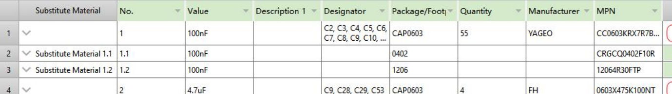
Figure 4-18: Sample substitute parts entry
Substitute parts can be set within HQDFM as well. These values will not be exported when using the export BOM function however.
3. Click the substitute part's cell in the Substitute Part column and click Set as substitute part.
4. In the new window, enter the row number of the primary part the selected part is substituting. Then click OK. The part will then have the label .1 attached. Subsequent substitutes for the same primary part will be labeled .2, .3, .4 and so on.
5. To convert a substitute part to a primary part, click the cell and select Set as primary part.
Once set, click next to proceed to the parts matching step.
There is no standard Bill of Materials format, and different EDA software export files with different headers and information. For HQDFM to detect and process the correct information, some BOM files may require simple pre-processing. HQDFM also supports built-in editing and the inclusion of alternative parts that can also take part in analysis.
4.6.1. Parts Matching Introduction
HQDFM's parts matching capabilities include footprint checking against HQDFM's database of over 5 million package libraries maintained by over 20 engineers. These package libraries contain information on the size and shape of the component body and pins, polarity and keep-out areas. With these libraries, HQDFM can perform footprint checking and complex DFA analysis on the entire BOM with one click.
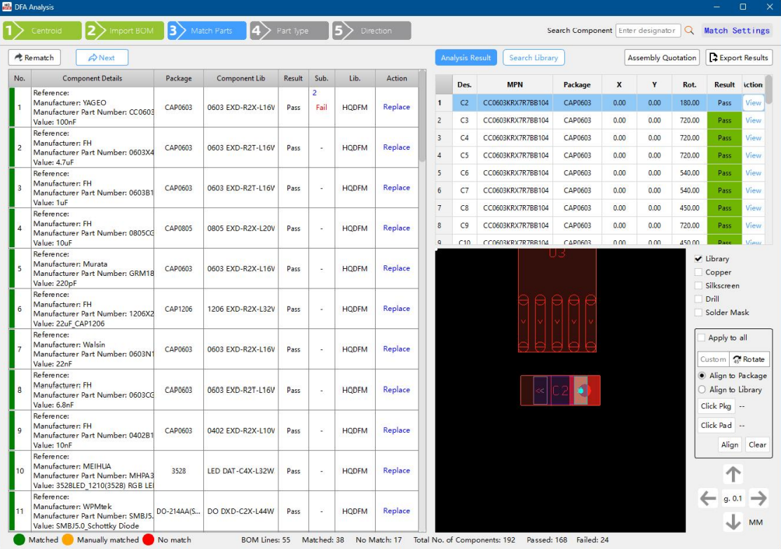
Figure 4-19: Match Parts stage
Component List: The left side shows a simplified BOM list with analysis result for primary and substitute parts, package information from the BOM and the corresponding HQDFM package library name. The total number of components and the number that passed and failed matching and analysis is shown on the bottom.
Designator List: Clicking a row in the component list will display a table of all the designators for that part on the top right side with their location and individual DFA analysis result.
Preview Window: Clicking a row in the designator list will cause the preview windowto zoom into the selected part's location on the PCB board. This window has an interface for individual component alignment and options to overlay PCB layers and supports pan and zoom actions.
Context Menu: Right-click to bring up the context menu.
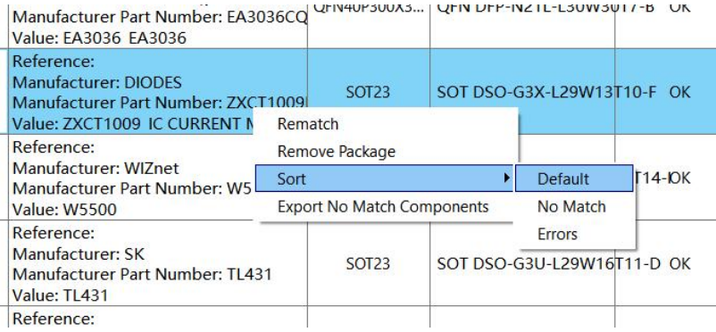
Figure 4-20: Match Parts context menu
a) Rematch: Repeat analysis on a single component
b) Remove Package: Remove the currently matched package
c) Sort: Sort the list with No Match or Error entries on top
d) Export No Match parts: Export a list of No Match parts
4.6.2. Perform Parts Matching
1. After BOM upload and verification, clicking the Next button will begin parts matching with HQDFM's database. Depending on the number of parts in the BOM, this may take a few seconds to complete.
2. Matched parts will be marked in green in the components list. If there is no match, they will be marked in red and require manual matching. Check the results of analysis for substitute parts by clicking the Sub. cell to bring up the Substitute Part Analysis Results window. The layout is similar to the interface for primary part verification.
3. For parts that failed analysis, click the row to bring up the designators on the top right section and view the individual violations. Click a designator to bring up the preview of the part on the PCB in the section below.
4.6.3. Centroid file editing for individual components
In the designator list, the X, Y and Rot. columns show the displacement in the x, y and radial directions respectively. The interface below the list can be used to move the component and change the rotation. Note that changes can only be made to the components shown in the designators list above. Select the appropriate component to make changes to that part.
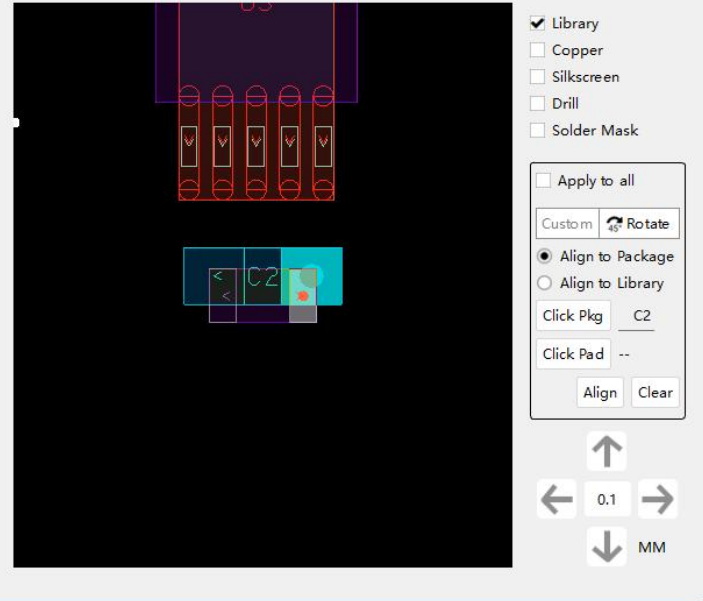
Figure 4-21: Move part interface
a) Toggle PCB layers: Click the check boxes to show the respective PCB layer in the preview window.
b) Move All checkbox: By default, the changes made in this interface only affect the selected part. By selecting this box, all instances of this part are affected by the changes.
c) Rotate: Click to rotate the part in 45 degree intervals to correct rotational errors.
d) Pad Alignment: Auto-align the part by selecting pads. Click a radial button to align using the entire component package or a single pin. Using a pin for alignment is useful for aligning through-hole parts since the pin must be at the centre of the plated hole. Click the part or part contact/pin until it is highlighted. Then click the Click Pad button and click the pad or pads to use for alignment. Then click align to move the part. Experiment with different pad combinations to centre the part with the PCB land pattern.
e) Arrow buttons: Moves the component by set increments to correct offset in the xy direction. The increment size can be changed by typing in the value in the middle of the arrows.
4.6.4. Manual Matching
A part may fail matching since the part MPN is not currently in the database. However, if the component has a common land pattern, you can search for the land pattern and manually assign it to the part.
a) Click the hourglass icon in the Package Library column to bring up the Search Library window on the right.
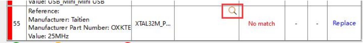
Figure 4-22: Hourglass icon for a part with no matching footprint
b) In this window, enter keywords such as package name, pin count and pitch to search for an existing package library that matches the part.
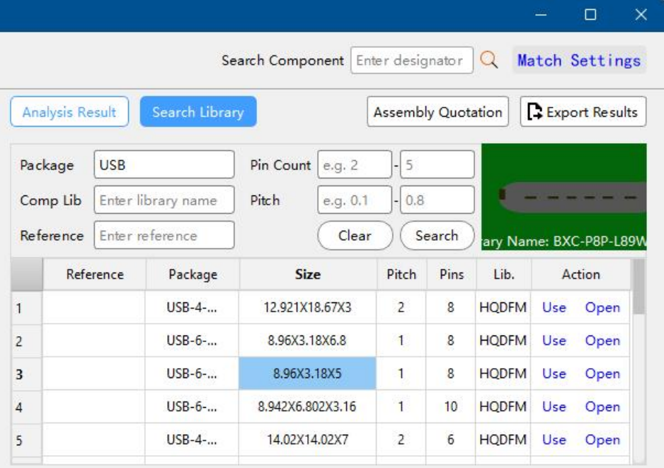
Figure 4-23: Search library interface
c) Click Use to apply and HQDFM will perform analysis on the new package.
If no suitable library exists, ignore the error and check the footprint matches the manufacturer's datasheet manually.
4.6.5. Assembly Quotation Calculator
The Assembly Quotation calculator can be opened by clicking the button on the top right corner of the Match Parts interface. Many PCB assembly houses calculate assembly fees based on the number and types of parts, the number of surface mount assembly sides and the pad count. The Assembly Quotation Calculator can summarize these values from the data provided to give you an overview of the design's assembly complexity, and can be exported to give to your assembly house or as part of an internal review process.
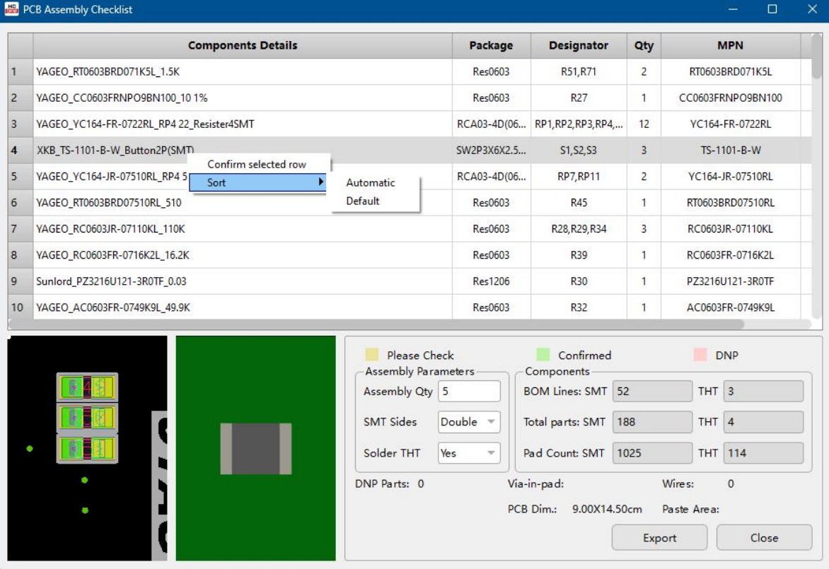
Figure 4-24: Assembly Quotation Calculator interface
1. Clicking a part will bring up a preview of the package library on the PCB on the left and the part on the right.
2. HQDFM will try to guess the assembly type based on the data available. If it is not sure, the cell will be filled in yellow and requires manual verification. Change the value by using the drop down box. If some parts donot need to be assembled (DNP), click the drop down box and change the value to DNP (Do not populate).
Figure 4-25: Assembly type selection
The assembly type information is used to calculate the number of surface mount and through-hole parts and pads for a single unit.
3. The Status column can be used to keep track and check-off verified parts. Click the drop down box to change the status. You can also right-click the row and select Confirm selected row to change the status to Confirmed directly.
4. Fill in the production parameters such as production quantity and the number of sides with surface mount parts. A summary of other assembly related information will be listed at the bottom.
5. Click the export button to export a spreadsheet file containing the BOM list and assembly parameters for reference.
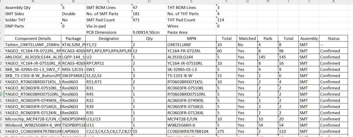
Figure 4-26: Assembly Quotation Output
Some IPC rules and DFA analysis methods depend on the component type. So it is important that all parts are assigned the correct component category. The Part Type stage allows users to assign the part type from a list.
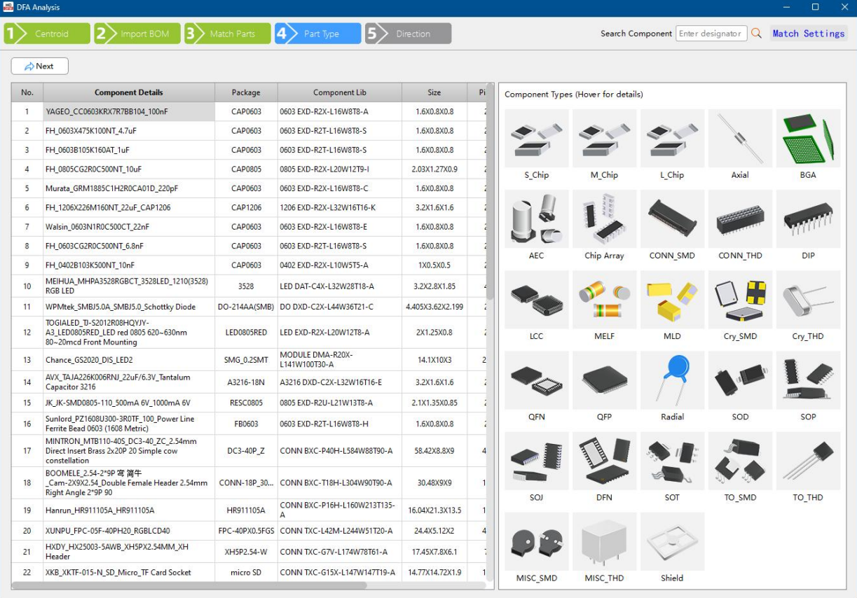
Figure 4-27: Part Type stage
4.7.1. Manual Assignment
Matched parts will have the Component Type automatically filled. Manually matched parts will require manual assignment.
1. The right side displays illustrations of the various component types and their code names for reference. Use this to identify the correct component type.
2. The selection will be saved so the next time the part is used, the last selected type will be assigned automatically.
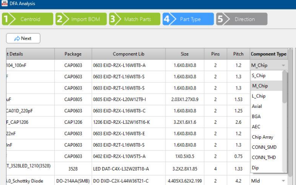
Figure 4-28: Component Type selection
Many DFA rules and design considerations are affected by the PCB panel's direction of travel, that is, how the panel is designed to enter automated assembly equipment. The direction of travel has a significant impact as a design is adapted for automated production.
Automated PCB assembly equipment use two conveyor belts of adjustable width to transport panels to and from different machines. The two edges of the panel that run across the conveyor belts, also known as transmission sides have clearance requirements and boards undergoing wave soldering have strict component placement guidelines.
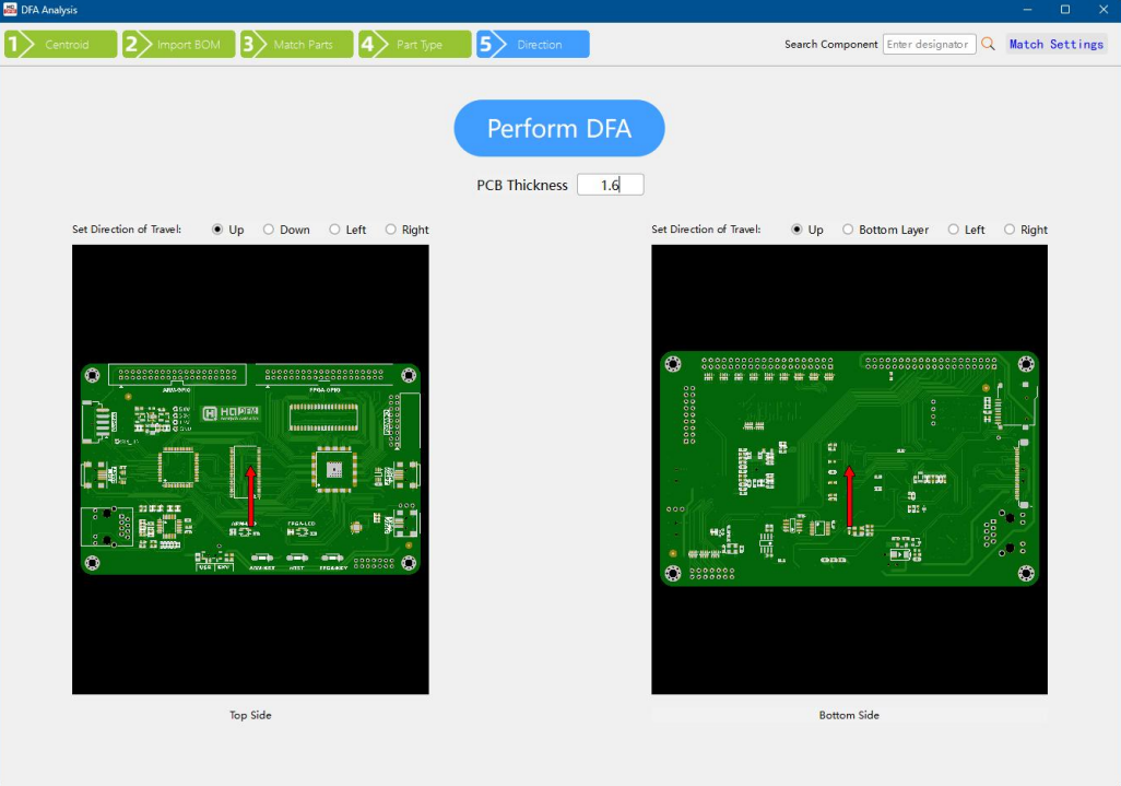
Figure 4-29: Direction stage
1. In HQDFM, the direction of travel can be set independently for both top and bottom sides. Click the relevant checkbox to change the direction of travel, using the red arrow for reference. Pointed tip marks the side that will enter first.
2. The board thickness can be also be entered to be used in PCBA height calculations. The default value is 1.6mm.
4.9.1. Component Spacing
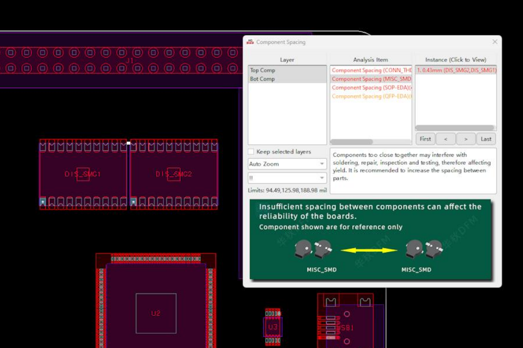
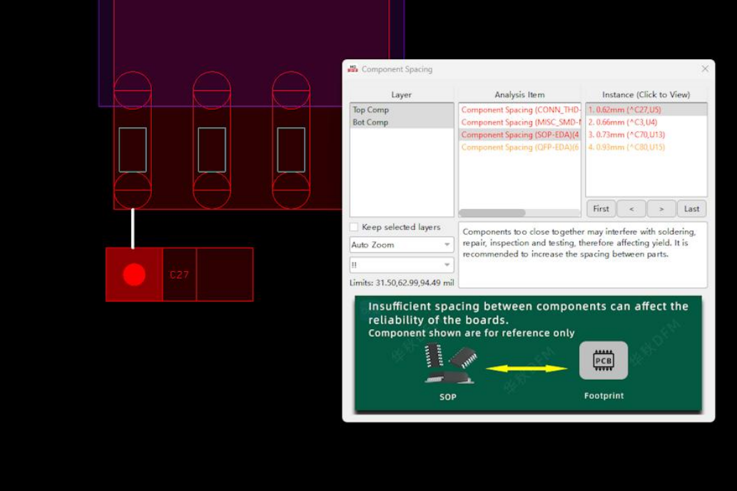
4.9.2. Comp-to-Board Edge
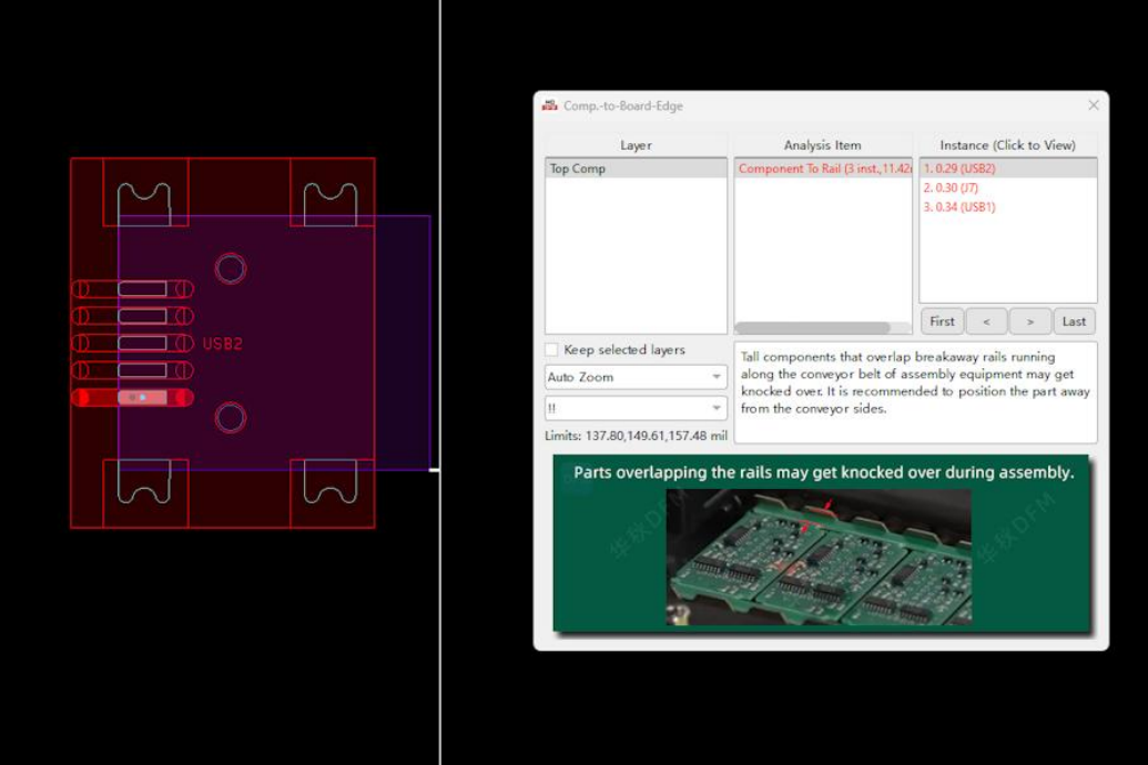
4.9.3. Comp Height Analysis
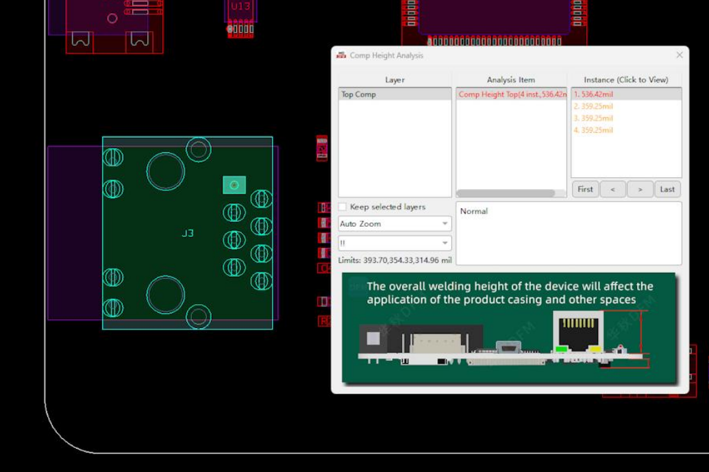
4.9.4. SMT Pad Analysis
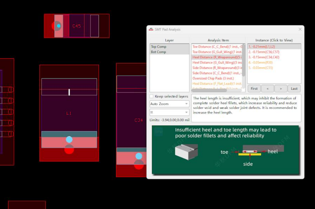
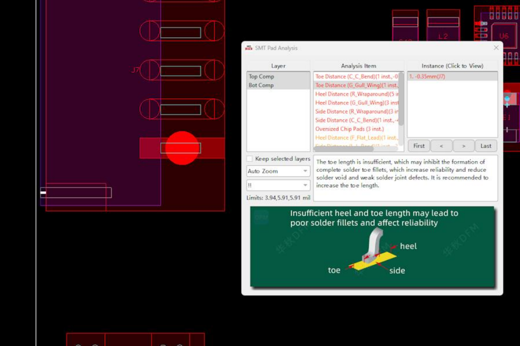
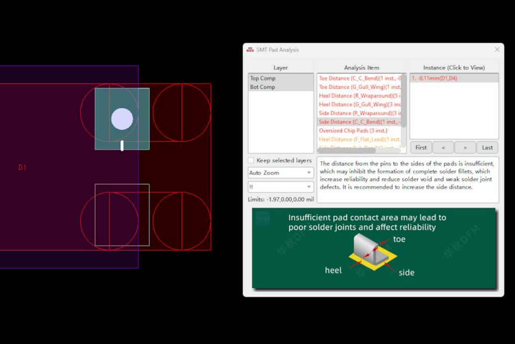
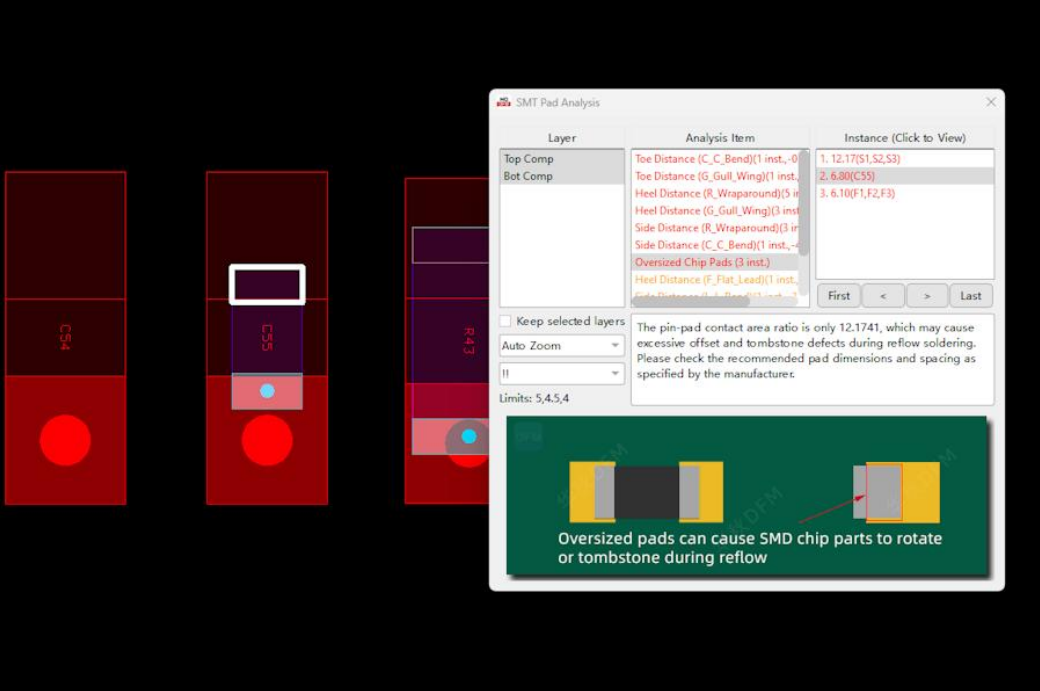
4.9.5. Chip Pads
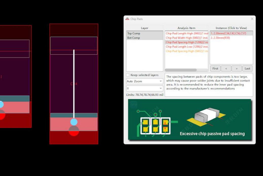
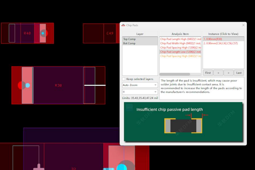
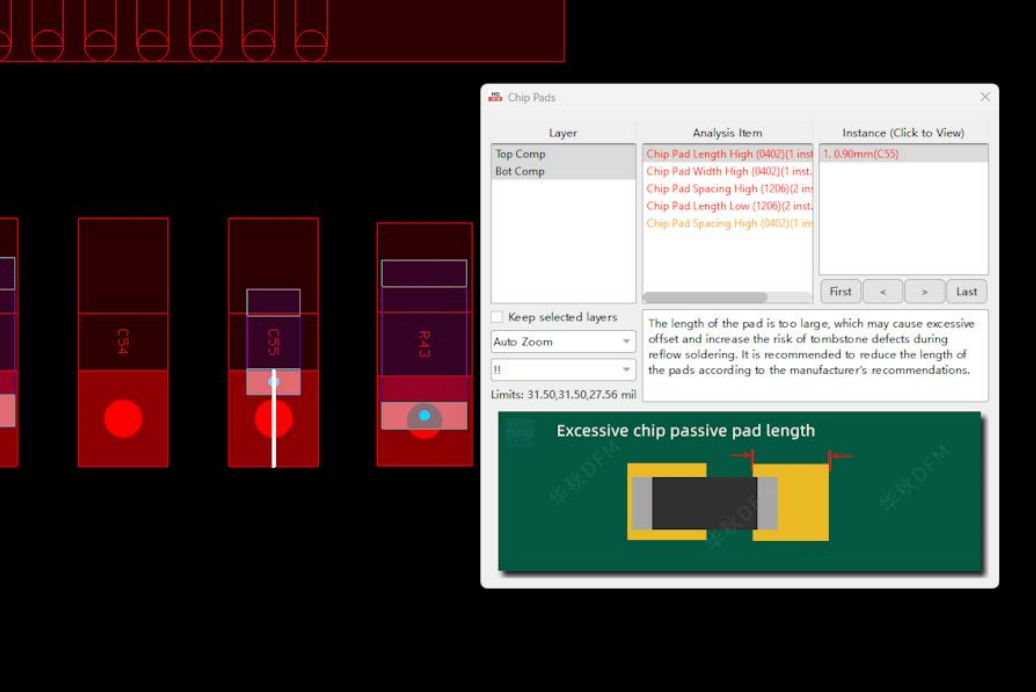
5.1.1. HQDFM's impedance calculator
HQDFM's impedance calculator is an advanced tool for calculating the trace impedance for multiple traces at the same time based on stack-up templates. The stack-up structure can be modified in the Stack-Up Manager on the left and the resulting structure can be saved in .json format.
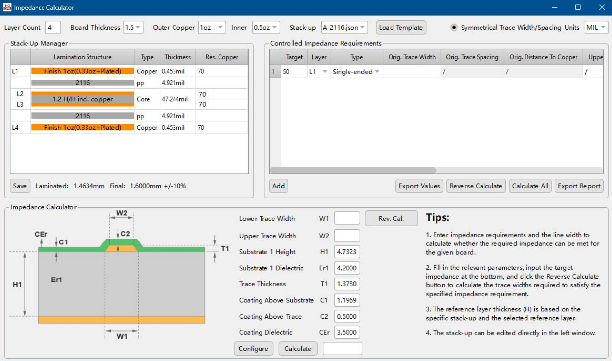
Figure 5-1: Impedance Calculator interface
The Compare Gerber Files tool allows users to quickly open and compare two sets of Gerber files and find differences between them.
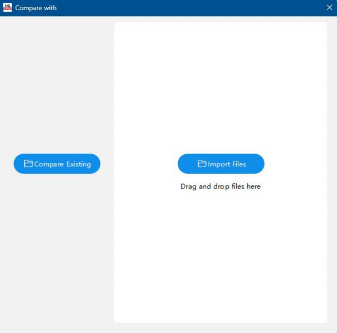
Figure 5-2: Compare Gerber Files tool interface
5.2.2. Steps: Compare Existing
Choose [Compare Existing] to compare files that have already been imported in HQDFM. This is useful if you need to compare layers in the same set of Gerber files or compare changes made in HQDFM to individual layers.
1. Import Gerber and drill files into HQDFM.
2. Open Compare Gerber Files tool and select [Compare Existing].
3. In the table, select the two layers to compare.
4. Click the plus sign to add more rows to compare other pairs of layers then click [Compare] to perform comparison.
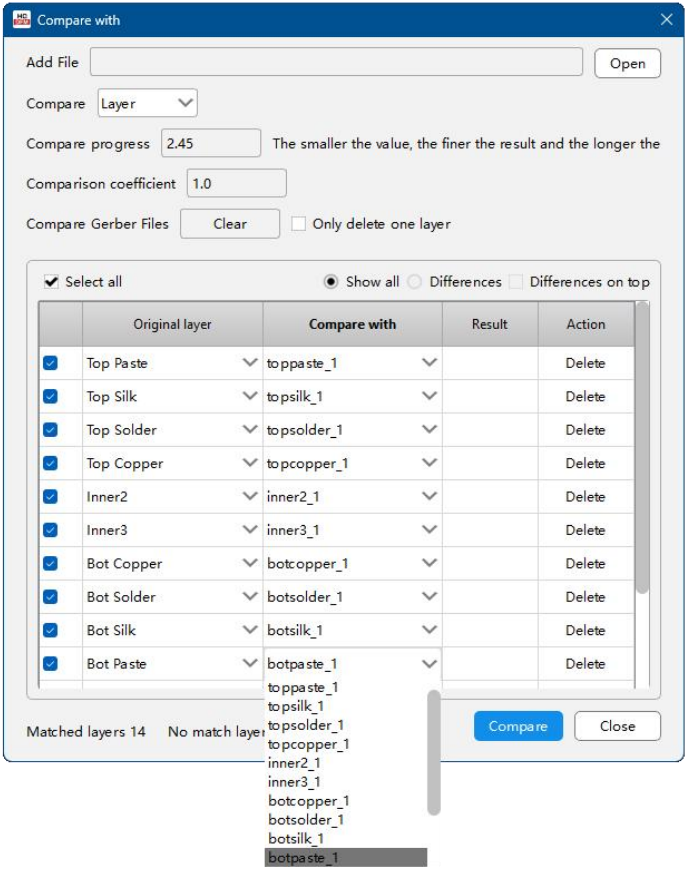
Figure 5-3: Comparing Gerber files in the same set of Gerber files.
5.2.3. Steps: Import Files
Select [Import Files] or drop files directly to compare the files already loaded in HQDFM with other Gerber files. This is useful for comparing different sets of Gerber files, e.g. different versions.
1. Import Gerber and drill files into HQDFM.
2. Open Compare Gerber Files tool and select [Import Files].
3. Select the individual Gerber files to add (archive files not supported). Successfully imported layers will be added to the table and temporarily added to the list of layers on the left of the workspace.
4. HQDFM will automatically try to match the layers according to layer type. If this is incorrect, change the assignment using the drop-down menu.
5. Select/deselect the layers as required and click [Compare] to perform comparison. Processing will take longer for larger files and more layers. Deselect some layers to speed up comparison.
5.2.4. Steps: Analyze differences
1. If differences were found, the result column will display Different and the [View] button will be red. Click [View] to display the inconsistencies in the workspace.
2. Click the Differences radial button to only display identified differences in the table.
3. When the Show All radial button is selected, check the Differences on top checkbox to display identified differences on top of the list.
4. Click [Clear] to clear the comparison results.
5. Click [Clear] with the checkbox ticked to delete the contents of the table.
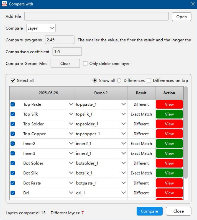
Figure 5-4: Compare Gerber Files result
5.2.5. Compare Gerber Files settings and interface
a) Compare: Choose to compare the whole layer, the elements within the board profile or a custom selection of elements. For the Custom option, draw the box section to be compared in the workspace. When successfully selected, the coordinates will be displayed on the right.
b) Compare progress: Change the Compare progress value. The higher the value, the faster the comparison but the level of detail will be not be as fine.
c) Comparison coefficient: The default value is 1. Change the pixel size for comparisons.
The Compare BOM Files tool can be used to find individual differences between BOM file versions with a convenient side-by-side view.
Steps:
1. Import the two BOM files to be compared and assign the headings if required.
2. Click [Compare]
3. Any differences will be highlighted in red on the right. Click the button in the Result column to jump to that row.
4. Clicking a cell will show the full contents on the bottom. The contents of any cell can be edited by selecting the cell and clicking [Edit] on the respective side. The preview field will turn white and the contents can be modified. Repeat the Compare action as required.
5. The modified BOM can be exported to save the changes using the [Export] button.
Compare BOM Files settings and interface:
a) [Import]/[Export]: Import BOM files for comparison and export modified BOMfiles.
b) Default: View the results in the same order as in the BOM file.
c) Differences: View the results with differences displayed on top.
d) Clear: Check this box to clear all imported data when exiting the tool.
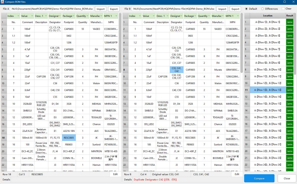
Figure 5-5: Compare BOM files interface
e) Row and Column: The selected cell's row and column will be shown here.
f) Details box: Error messages will be shown here such as duplicate designators, mismatching quantities etc.
g) [Close]: Closes the Compare BOM files window. If the Clear checkbox is not selected, the current session will be saved the next time you open the tool (but not if the project is closed).
Mistakes in the design file or export procedure may cause errors to appear in the production files that are not detectable in the EDA software. By using the Compare IPC Nets tool, shorts and opens can be identified by using IPC netlist files.
Steps:
a) You will need the IPC netlist (.ipc) file. Netlist export is supported by many EDA tools.
b) Import the Gerber and drill files and open the Compare IPC Nets tool. If the netlist file was imported with the Gerber files, you can also bring up the tool by first performing DFM Analysis then click the [Check] button next to the Opens/Shorts item.
c) Import the .ipc netlist file and click [Compare]. If the netlist file was imported with the Gerber files, the filename will automatically appear in the top field.
d) Any anomalies will be displayed in the table. Click an entry then click a PCB layer to zoom into the nets in the workspace. Objects in green are areas that are not connected that should be according to the IPC netlist. For shorts, the shorted nets will be shown and labeled in different colors.
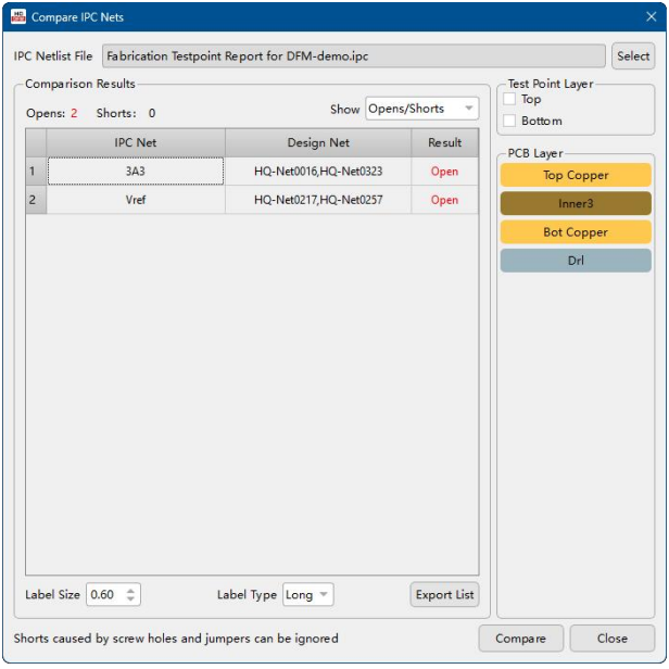
Figure 5-6: Compare IPC Nets interface
Other options:
a) Label Size: Change the size of the text label in the workspace.
b) Label Type: Change how labels are shown in the workspace or not shown at all.
Calculate the percentage copper coverage in circuit layers. Simply click calculate and the tool will calculate the copper area as a percentage of the total board area. This can be useful for gaining insights into the copper distribution between layers.
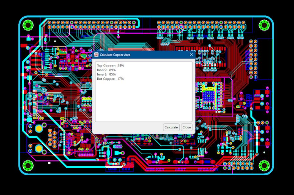
Figure 5-7: Compare Copper Area interface
The solder pad area calculator counts the number of surface mount and through-hole solder pads to give the solder pad count or pin count as otherwise known.
Click the Count button to automatically count all the pads. The View buttons on the side can be used to view and verify the pads which have been included in the calculation. Note that these pads are counted purely based on their layer properties and not whether they are included in the BOM or not.
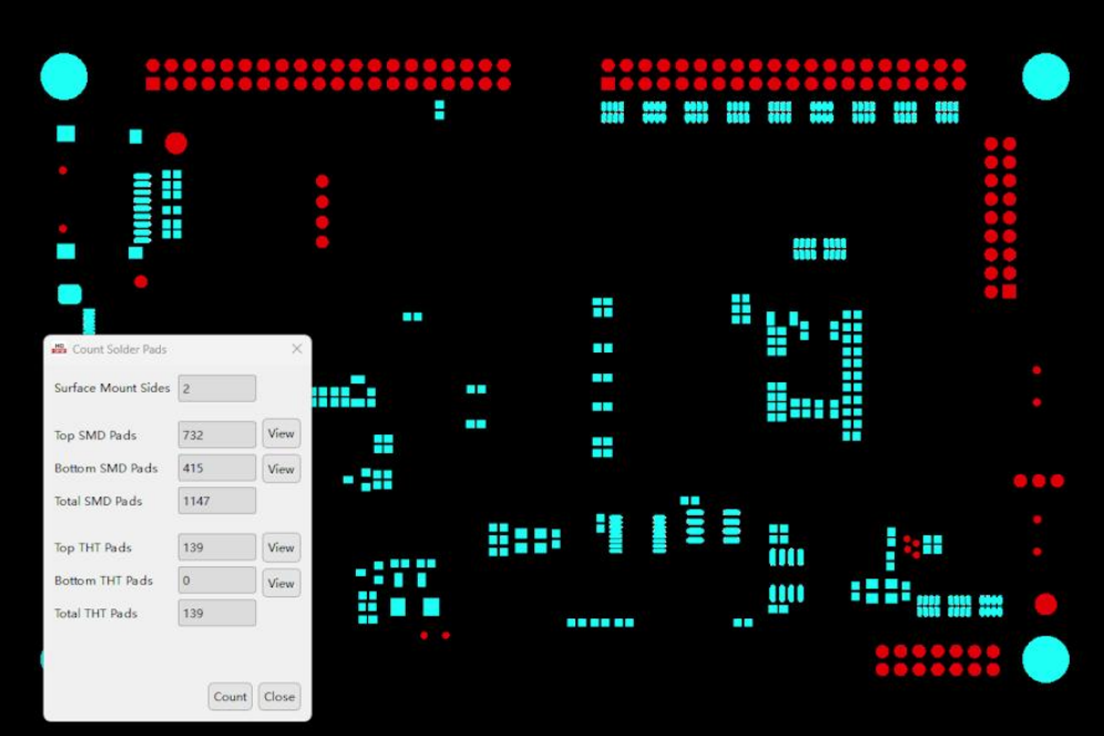
Figure 5-8: Count Solder Pads interface
Quickly find the location of any part on the board by importing the centroid file and specifying it's designator. You can also click the part in the list directly. If you have already imported the centroid file in the PCBA Analysis wizard then there is no need to import it again.
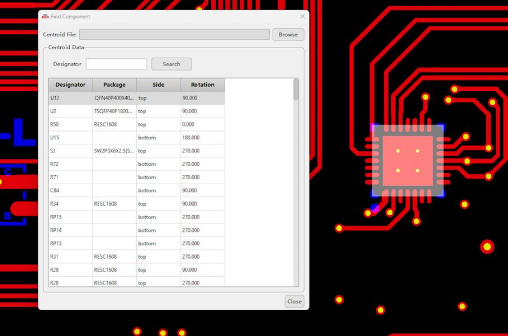
Figure 5-9: Find Component interface
5.8.1. PCB Panelization Tool Operation Guide
The panelization tool can be used to create panelized Gerber data with v-cuts, tabs, stamp holes, fiducial marks and breakaway rails quickly.
a) Ensure the profile has been created and in the panelization tool window, select the layer that contains the profile under the Basic Info section.
b) The Panel Outline field is the name of the output file that will be generated. The default value is "set" and can be changed by editing this field.
c) Choose the Panelization Type. You can choose from Regular, Rotate and Flip types.
d) Enter the number of board copies in the x and y directions and the preview on the right will update.
e) Enter the width in mm of any gaps between adjacent boards. By default these gaps will be hollow- check the connect outline box to place a filler piece in the gaps.
f) Select from preset breakaway rail configurations such as Left & Right, Top & Bottom, Four sides or custom values. Each width can be set individually or together by first changing the Width field then selecting the preset configuration.
g) The sizes of Fiducial Marks and tooling holes can be modified by changing the diameter value.
h) Click apply and the panel data will be generated in the workspace and panel dimensions will be updated.
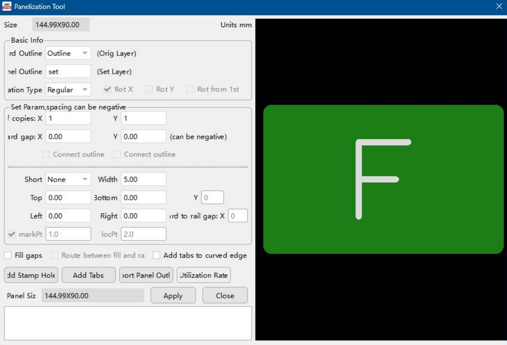
Figure 5-10: Panelization Tool interface
5.8.2. Panelization Tips
Rotate Panelization: Rotate panelization can be used to utilize panel space more efficiently for boards of a certain shape i.e. "L" shaped boards. Select the Rotate panelization mode and for the X or Y spacing then enter a negative value to move the boards closer together. Rotate panelization can also be used to move sides with overhanging components to the outer edges of the panel to prevent them from interfering with assembly.
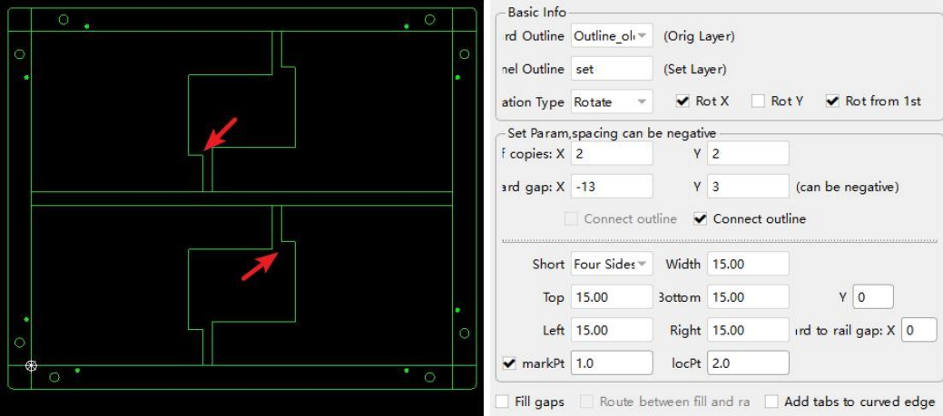
Figure 5-11: Setting up Rotate panelization for interlocking boards
Add Stamp Holes: Use the stamp hole tool to add tabs between boards lined with stamp holes. The number of holes, spacing and size can all be modified. Move the mouse to the spacing between boards. The outline of a tab with stamp holes will appear if tabs can be added in the area. Click to add the tab.
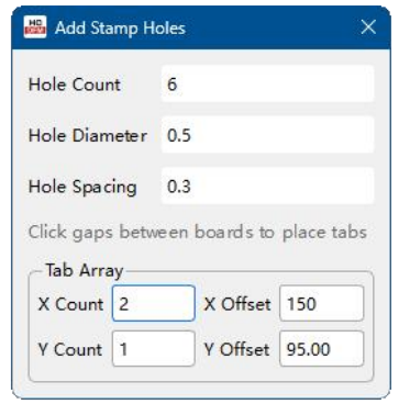
Figure 5-12: Add stamp holes tool interface
Select the outline and drill layer and the calculator will automatically select the appropriate routing tool size based on the width of the slots. To calculate the routing distance, first click the Analyze button to create the data layer which identifies breakaway rails from boards area. Click Generate to create the rou layer which contains route paths.
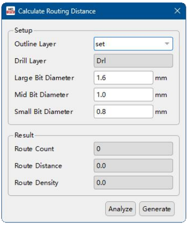
Figure 5-13: Calculate Routing Distance tool interface
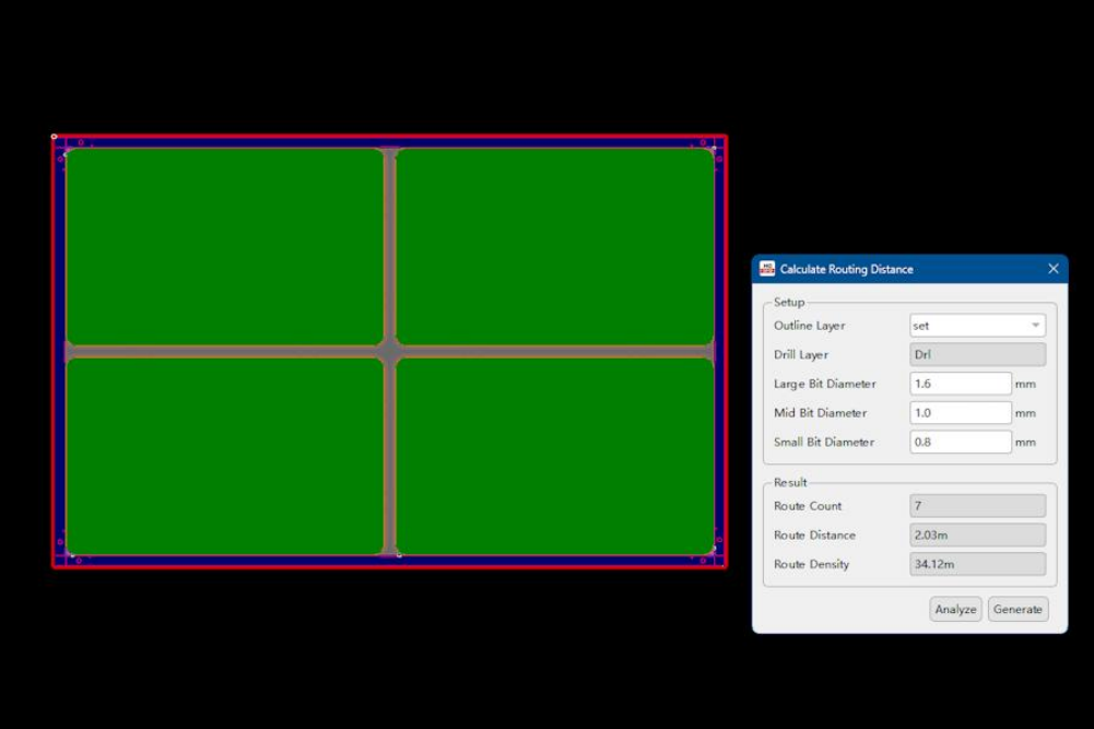
Figure 5-14: Routing and data layers
PCB raw substrate comes in fixed sizes from the manufacture. Before production, these panels need to be cut into smaller production panels for easier handling and the size of these panels is designed to maximize utilization rate and minimize waste.
PCB designers can use the utilization rate calculator to optimize the dimensions of their boards or panel for larger batch runs where waste can quickly accumulate.
Use the Utilization Rate calculator to calculate the utilization rate and the number of boards that can fit on raw panels of various sizes. The calculator will also suggest cut panel sizes and layouts. The greater the utilization rate, the less board material that goes to waste.
Utilization rate is defined as:
| Board area × no. of boards per standard panel |
| Raw panel area |
Ensure the board's dimensions have been defined or enter them on the calculator. Enter the number and size of test coupons if required. Maximum and minimum panel sizes can be modified as well. Calculations for multiple raw manufacturing panel sizes can be performed simultaneously by selecting the check boxes. Then click calculate to view the results.
The table shows the utilization rates for each configuration. Click a row to bring up the diagrams of the panels on the bottom. The cut panel design is displayed on the left and the raw panel is displayed on the right. Note that the boards in the cut panel will be fully routed out. If your design is to be produced as a panel, the dimensions of the panel should be entered in the calculator.
Click the FPC tab for the flexible PCB boards (FPC) calculator. The process is the same, however flex PCB substrate material typically produced in reels of a fixed width, therefore the width is limited but the length has greater freedom.
The effect on utilization rate is more apparent as board sizes get larger, which is more likely as boards are panelized.
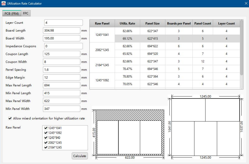
Figure 5-15: Utilization Rate Calculator
When the board is greater than half the width and length of the production panel, the panel can only accommodate one board, resulting in very high wastage which may incur additional costs. This can be reduced by designing a more rectangular board that is much longer than it is wide.
FAQ: High-Performance DFM Analysis for Advanced PCB Assembly & Fabrication
Q1: How does HQDFM improve impedance control accuracy for high-speed signal integrity?
Standard industry impedance tolerance is typically ±10%. HQDFM integrates a field-solver engine that simulates the etching factor and dielectric thickness variations during the pre-CAM stage. By identifying potential mismatches in differential pair spacing and reference plane continuity before the layout is finalized, engineers can lock in a ±5Ω tolerance. This significantly reduces signal reflections in PCIe 5.0 or DDR4/5 layouts, preventing costly re-spins due to signal integrity (SI) failures.
Q2: Can HQDFM detect hidden "Acid Traps" and "Copper Slivers" that standard DRC misses?
Yes. Traditional DRC (Design Rule Checks) often overlooks acute angles (less than 90°) and narrow copper islands. HQDFM performs a deep-level Manufacturing Analysis that specifically flags Acid Traps—where etchant collects and over-etches traces—and Copper Slivers that may peel off during soldering and cause intermittent shorts. By cleaning these up at the design stage, you ensure long-term reliability for mission-critical applications.
Q3: How does the "One-Click DFM Report" assist in reducing PCBA assembly costs?
HQDFM goes beyond the bare board. It analyzes Component Spacing, Solder Mask Openings, and Shadowing Effects for selective soldering or wave soldering. By identifying parts that are too close to the board edge or heavy thermal-sink components that require specialized thermal profiles, the tool helps you avoid manual rework. Case studies show using HQDFM to optimize BGA-to-Capacitor clearance reduced assembly NRE costs by an average of 15-20%.
Q4: Does HQDFM support advanced HDI (High-Density Interconnect) constraints like Microvias and Buried Vias?
Absolutely. For HDI Tier 1, 2, and 3 designs, HQDFM validates the aspect ratio of laser-drilled microvias (typically keeping it below 1:1 for plating reliability). It also checks for stacked vs. staggered via alignment and annular ring integrity. If a design exceeds manufacturing capability (e.g., an annular ring < 2mil), HQDFM triggers a high-risk alert before the prototype phase.
Q5: How does the tool handle multi-format CAD data like Gerber X2, ODB++, and Kicad files?
HQDFM features a robust intelligent parsing engine that supports direct import of ODB++ (the industry gold standard), Gerber RS-274X, and Kicad files (.kicad_pcb). Unlike basic viewers, it reconstructs the netlist and stack-up information, ensuring that the "Physical Design" matches the "Electrical Intent," eliminating the #1 cause of manufacturing delays.
Q6: Can HQDFM help in selecting the most cost-effective surface finish (ENIG, HASL, OSP)?
Its Cost Estimation module evaluates design complexity against surface finishes. For example, if your design has 0.4mm pitch BGA components, HQDFM will recommend ENIG over HASL to ensure pad flatness (planarity), preventing "black pad" issues or tombstoning during reflow.
Q7: How does the software ensure compliance with IPC-A-600 and IPC-2221 standards?
HQDFM’s rule deck is built upon IPC Class 2 and Class 3 standards. It automatically checks for minimum trace width/spacing based on copper weight (e.g., requiring wider gaps for 2oz heavy copper boards) to meet IPC-2221 thermal requirements. This ensures your board is not just "manufacturable," but "compliant" for global markets.