
 NextPCB Capabilities
Printed Circuit Boards
NextPCB Capabilities
Printed Circuit Boards
 PCB Assembly
 Layer Buildup
 SMD-Stencils
 PCB Design-Aid & Layout
 Mechanics
 Quality
 Drills & Throughplating
 Factory & Certificate
 PCB Assembly Factory Show
Certificate
PCB Assembly Factory Show
Certificate
Support Team
Feedback:
support@nextpcb.com


In the world of PCB design, especially when you are ready to jump out of simple hobby projects and start taking on commercial hardware development, the first watershed you often encounter is: should this board use 2 layers or 4 layers? Actually, in commercial hardware development, a 4-layer board is already the default starting point, not an upgrade option.
Many people's intuitive reaction is "if you can use 2 layers, never use 4 layers" to save money, after all. In many cases, this intuition is correct, but reality is often more complex than this. If you are stingy where you shouldn't be, those twenty or thirty dollars saved might turn into lingering ripple noise during debugging, EMI tests that simply won't pass, or even the nightmare of a board running perfectly in the lab but crashing inexplicably in the field.
This article isn't going to recite textbook theories to you. I want to combine our decades of experience in the EMS electronic manufacturing field to talk about the essential structural differences between the two, and when you should decisively choose to "upgrade". Most importantly, we will discuss real prototyping costs without any gimmicks.
Before diving into a deep comparison, let's align our concepts. The PCB "layers" we often talk about actually refer to the conductive copper layers inside the circuit board. Each layer can be used to route signals, draw power lines, or pour large areas of copper as a Ground Plane.
The most common 2-layer board is like a sandwich: the top and bottom are copper layers, and in the middle is a layer of FR4 insulating substrate. A 4-layer board inserts two additional layers of copper inside this sandwich. These two inner layers are laminated together through a high-temperature and high-pressure process, which is why the processing cost of a 4-layer board is higher and the lead time is slightly longer.
Looking at the physical structure, a 2-layer board is very straightforward: top layer routing, bottom layer routing, with about 1.6mm of FR4 core material in between. For the vast majority of basic projects, this is entirely sufficient.
If you are working on a simple microcontroller project (like basic control boards for Arduino, ESP32, or STM32), standard LED drivers, power modules under 10W, or low-frequency audio circuits, a 2-layer board is the most cost-effective choice. As long as the signal frequency stays below 50MHz and you don't have extremely demanding electromagnetic compatibility (EMI) requirements, a 2-layer board is completely up to the task.
But the shortcomings of a 2-layer board are equally obvious, mainly reflected in "space competition." Because there are only two routing layers, signal lines, power lines, and ground lines must fight for seats on just two surfaces. It's hard to dedicate a complete layer to act as a ground plane, which causes the return path to become very long and uncontrollable. As the design becomes more complex, especially when you use BGA or high-pin-count QFP packages, you may have to make the board very large or abuse vias just to bypass dense pins, which actually increases design difficulty.
Since we mentioned design details and space competition, many engineers are often curious: With a fixed thickness, can a 2-layer board actually achieve impedance control? The answer is yes, but it requires very careful parameter settings, and it often further compresses the already tight routing space. To provide you with a more intuitive reference, we share a few common practical cases here:
When the copper foil thickness of the Top and Bottom layers of a 1.6mm thick 2-layer board is 1oz, and the trace width and copper pour spacing are set to 12mil and 4mil respectively, the impedance is approximately 53.39Ω. The 50Ω impedance design parameter scheme (1) for a 1.6mm thick 2-layer board is shown in Figure 1.
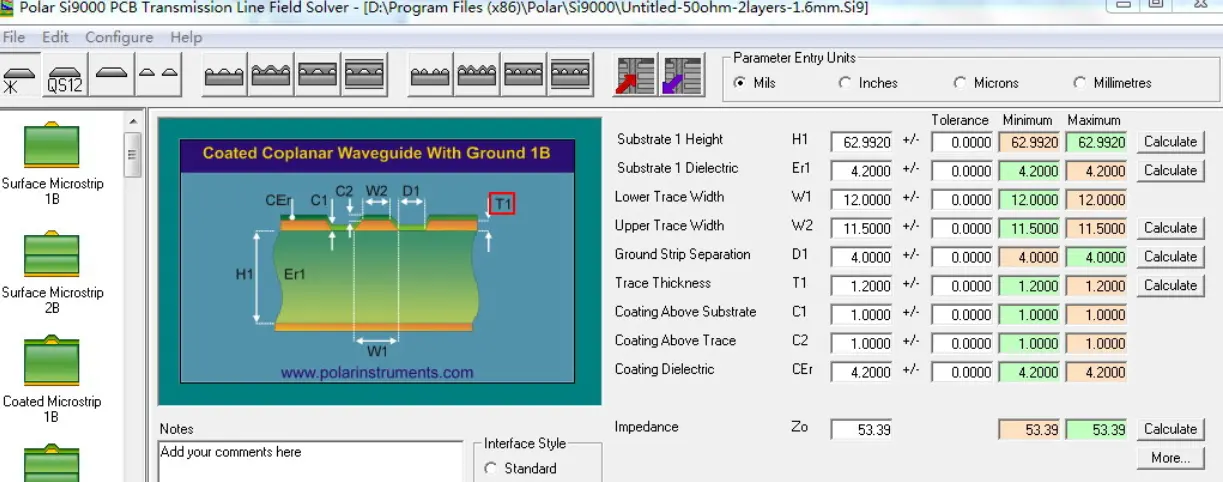
Figure 1: 50Ω impedance design parameter scheme (1) for a 1.6mm thick 2-layer board.
When the copper foil thickness of the Top and Bottom layers of a 1.6mm thick 2-layer board is 1oz, and the trace width and spacing are set to 10mil and 4mil respectively, the impedance is approximately 55.64Ω. The 50Ω impedance design parameter scheme (2) for a 1.6mm thick 2-layer board is shown in Figure 2.
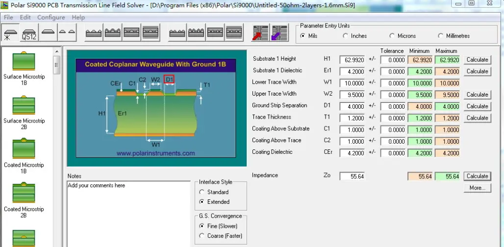
Figure 2: 50Ω impedance design parameter scheme (2) for a 1.6mm thick 2-layer board.
From Figure 1 and Figure 2, it can be seen that when designing impedance, the trace width of a 2-layer board will be much wider than that of a multi-layer board (4 layers or more). If a 2-layer board is to have a 50Ω impedance design, the surface layer can use a 1oz copper foil thickness, and the trace width and copper pour spacing can be set to 12mil and 4mil respectively. The resulting impedance is 53.39Ω, which meets the requirement of 50 × (1 ± 10%) Ω.
Knowledge Extension: Actual Impedance When Designing a 10mil Trace Width on a 1.6mm Thick 2-Layer Board
For a 2-layer board with a thickness of 1.6mm, the copper foil thickness of its Top and Bottom layers is 0.5oz. When both the trace width and spacing are set to 10mil, the impedance is approximately 81Ω. When engineers use design software for PCB design in the introductory stage, if they do not set the trace width and spacing, nor pay attention to impedance, they are using the default parameters of the design software. If the default parameters are 10mil for both trace spacing and trace width, and no changes are made when designing a 1.6mm thick 2-layer board with 0.5oz copper pour on both Top and Bottom layers, the actual impedance range after processing will be 80~85Ω. In reality, the manufactured thickness of a 2-layer board will be less than 1.6mm, roughly 1.4~1.55mm. Here, for the sake of demonstration, the nominal thickness of the 2-layer board is chosen to be 1.6mm.
Through the impedance calculation of the design software, the actual impedance is derived as 81.73Ω, as shown in Figure 3, which is not the expected 50 × (1 ± 10%) Ω.
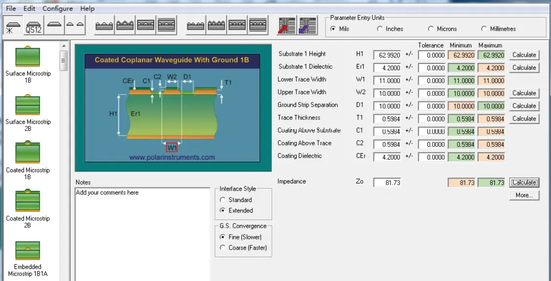
Figure 3: Actual impedance calculation result for a 10mil trace width on a 1.6mm thick 2-layer board.
Because design software defaults to this rule, designs without special adjustments will result in an impedance of around 81.73Ω. The reason signal line routing is not designed according to a 50Ω impedance is that in scenarios where signal integrity is not considered, this design can already meet usage requirements. This also explains why many engineers who have designed 2-layer boards for a long time still do not know what impedance really means, or even mistakenly believe that impedance design is useless.
In most 2-layer board designs, plug-in components and pin headers are used. To ensure sufficient insulation distance between the copper pour and the plug-in components, engineers usually design a separate distance between the copper pour and the signal line network (Distance D1 in Figure 3) of 15mil. With this, the impedance of the 10mil signal line will change from 81.73Ω to 92.25Ω.
2-layer boards rarely use impedance design because when doing so, the ratio of trace width to spacing will limit PCB routing. However, sometimes the need for impedance design is unavoidable. For example, when 4G modules, GPRS modules, Wi-Fi modules, etc., are used as optional communication adapter plug-ins, if the number of differential pairs does not exceed 2 groups, you can attempt to implement impedance matching. As long as the layout space is sufficient, using a 2-layer board can be considered. But if the number of differential pairs is large, you need to use a PCB design of 4 layers or more.
(1) The differential impedance design is 90 × (1 ± 10%) Ω. In terms of PCB design, the trace width and spacing are set to 12mil and 4mil respectively; the spacing between the copper pour and the network is set to 10mil. The resulting impedance is approximately 92.19Ω, as shown in Figure 4.
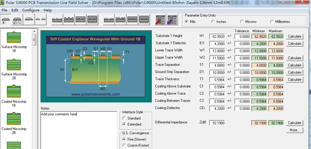
Figure 4: 90Ω differential impedance design parameter scheme (1) for a 1.6mm thick 2-layer board.
(2) The differential impedance design is 90 × (1 ± 10%) Ω. In terms of PCB design, the trace width and spacing are set to 20mil and 8mil respectively; the spacing between the copper pour and the network is set to 8mil. The resulting impedance is approximately 93.63Ω.
2-Layer Board Design Case: A GPRS/4G module supports three-network (Mobile, Unicom, Telecom) communication. The circuit design of the physical board is shown in Figure 5.
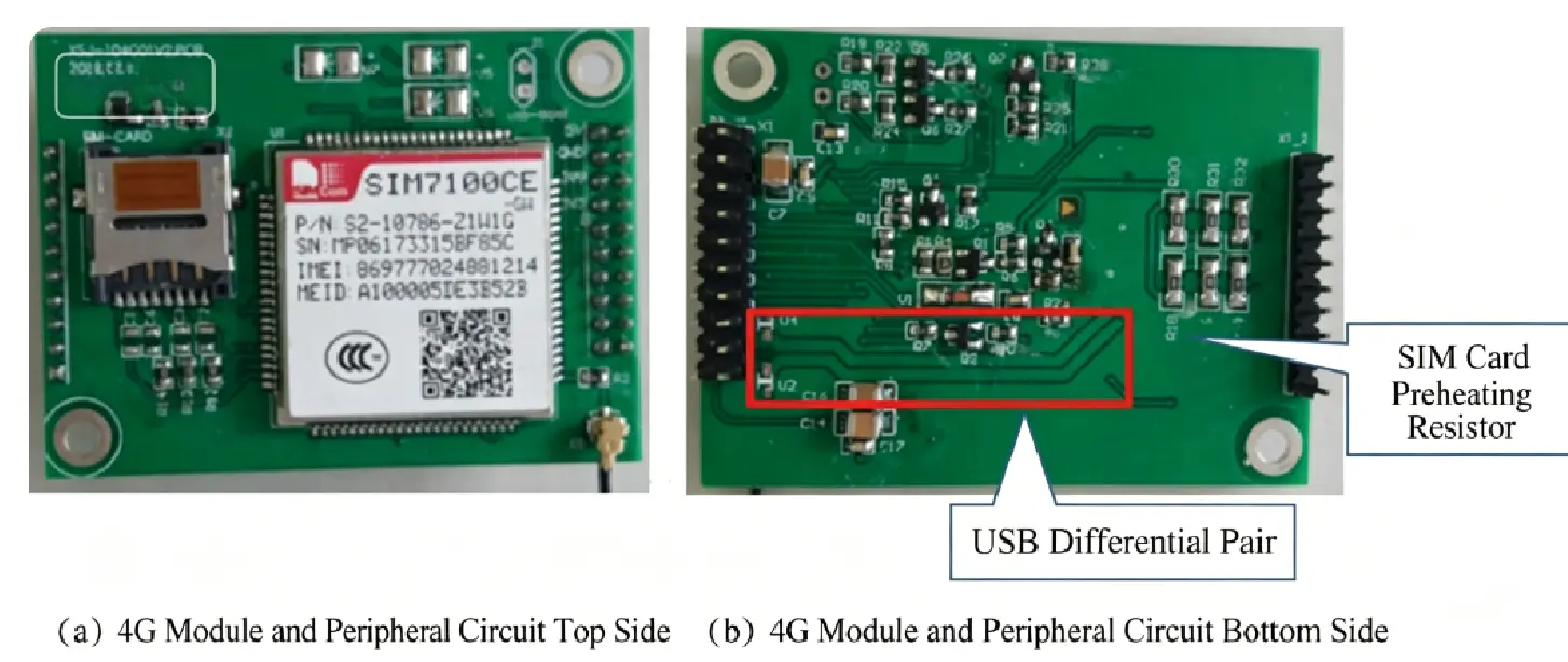
Figure 5: Circuit design of the physical board for a 4G module on a 2-layer PCB.
When impedance is discontinuous, the signal can be improved by connecting a matching resistor in series, as shown in Figure 6.
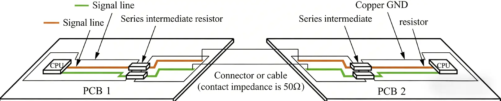
Figure 6: Using series matching resistors to improve signal quality when facing impedance discontinuities between two PCBs.
This design is not optimal; it is just to make the designer aware that even 2-layer boards should be designed according to standardized impedance matching. In fact, for a differential pair signal line to pass from a 4-layer PCB with an impedance design through a connector to another 2-layer PCB, this process will inevitably experience impedance discontinuity. Engineers who understand signal matching and transmission line knowledge will mostly design according to standard impedance matching. Yet, even knowing how to design it structurally, it may still be impossible to completely achieve continuous impedance, and issues with signal reflection and imperfect waveforms will persist.
To address these problems, an effective improvement measure is to connect a small resistor in series on the connector signal line, which can maximize the mitigation of impedance discontinuity impacts. Suppose the signal line differential pair of both PCBs is designed for 90Ω impedance, and the connector's impedance is 50Ω (the impedance varies among connectors and should be determined based on manufacturer data). To make the impedance transition more continuous and reduce signal reflection, we choose to insert an intermediate resistor in series with a value of (90−50)/2+50=70Ω. This creates a "90Ω − 70Ω − 50Ω" step relationship.
If you use Cadence Sigrity high-speed circuit signal simulation software to simulate this circuit, you will find that the waveform after the "90Ω − 70Ω − 50Ω" stepped treatment is more perfect than the waveform of a direct "90Ω − 50Ω" connection. There is one point that needs special attention here: when using this method to improve the circuit, you must consider the input impedance of the receiving end chip. If the input impedance forms a voltage divider with the series resistor on the signal line, it will affect the signal's logic judgment. Therefore, the value of the series resistor needs to be changed to 0Ω. While this method can mitigate the issue, it is fundamentally a remedial workaround rather than an optimal structural design. Electronic circuit design tricks are like a double-edged sword; they might perform excellently in the application of Product A, but may trigger serious problems in Product B due to being unsuitable. Therefore, once electronic hardware engineers master a series of circuit design techniques, they still need to flexibly adjust and apply them according to the actual situation.
As demonstrated by these stack-up and impedance cases above, although a 2-layer board can barely handle impedance design, doing so severely limits routing space and flexibility, leaving a very low design tolerance for error. This naturally leads to our next core question—
Although a 4-layer board is a bit more expensive, its structural design is actually meant to solve performance ceiling issues. The standard 4-layer board stack-up (Signal / Ground / Power / Signal) is a widely recognized configuration scheme in the industry.
Placing the ground plane on the second layer, right next to the top layer signals, provides an extremely low-impedance return path and offers effective electromagnetic shielding. If your circuit contains clock signals exceeding 100MHz, or involves mixed analog and digital signals, the advantages of a 4-layer board will shine through—the noise from the digital section will not easily couple to the sensitive analog end.
More objectively, if your design includes any of the following scenarios, it is recommended to prioritize a 4-layer board:
In engineering R&D, budget evaluation is a crucial link. Since a 4-layer board involves more lamination processes, inner layer etching, and stricter Automated Optical Inspection (AOI), its processing cost is naturally higher than that of a 2-layer board. However, at NextPCB, with process optimizations, this price gap is gradually narrowing.
Taking the common 100x100mm specification as an example, the prototyping fee for 5 pieces of a 2-layer board is usually around $5 to $15 USD (depending on surface treatment). The 4-layer board of the same specification is around $30 to $60 USD. Although the cost has increased from a unit price perspective, looking at the entire R&D cycle, a more stable hardware performance and a shorter test reproduction cycle can often offset this initial investment. If you end up spending two extra days debugging because of a 2-layer board, this price difference is essentially already offset.
> Know Custom PCB and PCBA Cost Analysis: How to Optimize Design and Reduce Expenses
Additionally, the cost of "impedance control" needs to be factored in. When dealing with high-speed USB 3.0, HDMI, or DDR memory routing, impedance matching is a mandatory process. In the prototyping stage, this usually incurs a testing fee of several tens of dollars. The engineering team at NextPCB will assist in verifying stack-up parameters (including copper thickness, dielectric thickness, and trace width) to ensure the final board meets the impedance targets defined in your design.
When selecting the number of layers, you shouldn't only consider technical specifications; you must also weigh time costs.
If you need to spend a massive amount of effort avoiding signal interference within the confines of 2 layers during the routing phase, and still face potential signal integrity risks, then the design certainty brought by a 4-layer board aligns much better with the logic of engineering development. Our advice is: if the design will ultimately be introduced to the market and enter mass production, adopting a 4-layer structure in the prototype stage is not only more robust but also better simulates the operating state of the final product.
When placing an order at NextPCB, simply specify the stack-up definition in the system. The factory will strictly execute layer sequence alignment and electrical performance testing to ensure the delivery quality of the prototype boards.
Get a specific cost reference:
If you are already struggling with whether a 2-layer board can get the job done, you can actually just drop your Gerber files into the quoting system, see the actual price difference for 4 layers, and then make your decision. The NextPCB platform will provide a transparent prototyping quote, and the engineering team will offer a free DFM check to help you uncover potential design risks before manufacturing.
Read More: How to Design a 4-Layer PCB Stackup for High-Speed Digital Circuits
Get an Instant Quote for PCB Prototypes →
Q: Can I add a ground plane to a 2-layer board to improve performance?
Yes, and you should — but it's not the same as a dedicated ground plane layer. A ground pour on a 2-layer board fills unused copper areas with GND-connected copper, which helps, but it's interrupted by signal traces and vias. The return current paths are less predictable than a solid internal ground plane on a 4-layer board. It's a useful improvement for 2-layer designs, just not equivalent.
Q: Will my 2-layer board pass FCC/CE certification?
It depends entirely on your design and operating frequencies. Many simple products with 2-layer boards pass without issue. But if you have components running at high clock rates, fast edge transitions, or wireless functionality, a 4-layer board gives you significantly more margin. The cost of failing an EMC test and having to respin the board far exceeds the $40 saved by not going to 4 layers.
Q: Is a 4-layer board harder to design?
Mostly no — it's actually often easier. Having dedicated ground and power planes means less time spent routing power distribution and managing return paths. The main extra step is defining your stackup upfront, which takes about 5 minutes in KiCad or Altium. The routing itself becomes more straightforward because signals and power aren't competing for the same layer space.
Q: Do all PCB manufacturers support 4-layer boards?
All major online PCB manufacturers support standard 4-layer boards as a baseline offering. Advanced configurations (6-layer, 8-layer, blind/buried vias, controlled impedance) vary by manufacturer. For prototypes, confirm that your chosen manufacturer supports your specific requirements before uploading files.
Q: What's the minimum trace width for inner layers on a 4-layer board?
Standard manufacturing supports 0.1mm (4mil) trace width and spacing on inner layers, though 0.15mm is more reliably achievable across all manufacturers. Inner layers can run tighter traces than outer layers in some cases because there's no surface plating step. Check your manufacturer's capability table before designing to the limit. >> View NextPCB Capabilities
Q: Should I use blind or buried vias on my 4-layer board?
For most designs, standard through-hole vias are sufficient and keep costs lower. Blind vias (connecting only outer to inner layers) and buried vias (connecting only inner layers) are used in high-density designs where board real estate is extremely tight — typically smartphones, wearables, or advanced industrial boards. Avoid them for standard prototypes unless genuinely necessary; they add meaningful cost and complexity.
Q: My rev1 2-layer board has noise issues. Should I go to 4 layers for rev2?
Probably yes — but first confirm the noise source. If the issue is a missing decoupling cap or a poorly routed power trace, fixing those on a 2-layer rev2 might be enough. If the issue is fundamental (ground bounce, insufficient return path continuity, EMI from fast edges), a 4-layer board with a solid ground plane will address it structurally. It's worth spending 30 minutes with a scope and power analyzer to diagnose before committing to a respin.
>> Images in this article are sourced from: Chen, T. (2026). Illustrated Handbook for Entry-level Electronic Hardware Engineers (Work Guidance). People's Posts and Telecommunications Press.
Still, need help? Contact Us: support@nextpcb.com
Need a PCB or PCBA quote? Quote now


 Surface

