NextPCB Capabilities
 PCB Assembly
 Layer Buildup
 SMD-Stencils
 PCB Design-Aid & Layout
 Mechanics
 Quality
 Drills & Throughplating
 Factory & Certificate





How PCB Fabrication Works, What to Check, and How to Choose a Manufacturer (2026)
If you're sourcing circuit boards from China, you're one of a very large number of hardware teams doing the same thing — the country fabricates the majority of the world's printed circuit boards. That scale is exactly what makes the decision harder, not easier: more manufacturers, more marketing claims, and more variation in what "quality" actually means from one supplier to the next.
This guide covers how PCB fabrication actually works, what a modern China-based factory looks like on the inside, which certifications are worth checking (and which ones aren't universal), a 2026 shipping change that affects EU-bound orders, and a practical checklist for evaluating a manufacturer before you commit a production run to them.
What Is PCB Fabrication?
PCB fabrication is the process of turning a design file (your Gerber files, drill data, and stackup) into a physical bare board — before any components are placed on it. At a high level, the process runs through:
- Inner layer imaging and etching — copper is patterned onto each internal layer according to your design.
- Layer stacking and lamination — layers are pressed together under heat with prepreg bonding material.
- Drilling — holes and vias are mechanically or laser-drilled through the stack.
- Plating — copper is deposited through the drilled holes to create electrical connections between layers.
- Outer layer imaging and etching — the same imaging process is repeated on the outer copper layers.
- Solder mask and silkscreen — protective coating and component labeling are applied.
- Surface finish — a finish (HASL, ENIG, OSP, etc.) is applied to exposed copper pads to protect them and prepare them for soldering.
- Electrical testing and inspection — boards are tested for opens and shorts before shipment.
For a deeper walkthrough of each stage, see the full PCB manufacturing process guide.
Why So Much PCB Fabrication Happens in China
A few structural factors explain why China handles such a large share of global PCB production:
- Supply chain density. Copper-clad laminate suppliers, chemical suppliers, drilling and plating equipment vendors, and component distributors are often located within the same industrial regions, shortening lead times for raw materials.
- Manufacturing scale. Large facilities can run both small prototype batches and high-volume production on the same equipment base, which keeps quick-turn services commercially viable alongside mass production.
- Vertical integration. Many manufacturers combine bare-board fabrication with SMT assembly and, increasingly, component sourcing — reducing the number of vendors a hardware team has to coordinate.
None of this automatically means any given supplier is a good fit for your project — capability, quality process, and communication still vary widely between manufacturers. The sections below cover what to actually check.
Inside a Modern China PCB Factory
Rather than describe this abstractly, here's what one such facility looks like in practice, using NextPCB's own factory as an example.
NextPCB's headquarters and PCB fabrication operations are based in the Shenzhen Special Economic Zone, with a PCB industrial park covering approximately 166,666 m². Equipment on the fabrication side includes imported high-precision drilling machines (minimum hole diameter 0.15 mm), automated pattern plating lines, and LDI (laser direct imaging) exposure equipment capable of 3/3 mil minimum line width and spacing. Every board is 100% electrically tested before shipment using flying-probe testers.
On the assembly side, NextPCB operates two SMT factories totaling roughly 15,000 m², running 27 automated Siemens SMT lines with a combined daily capacity of more than 95 million solder joints, supported by SPI, AOI, and X-ray inspection.
In 2026, NextPCB brought a new $210 million smart manufacturing base online in Jiangmen — a roughly 60-acre facility that integrates a 20,000 m² component warehouse, a 65,000 m² PCB flexible manufacturing center, a 40,000 m² PCBA assembly facility, and a 10,000 m² quality assurance and testing center under one roof. Housing component sourcing, fabrication, and assembly in a single site is specifically meant to cut the transfer time between those stages, which is usually where delays accumulate on a multi-vendor supply chain.
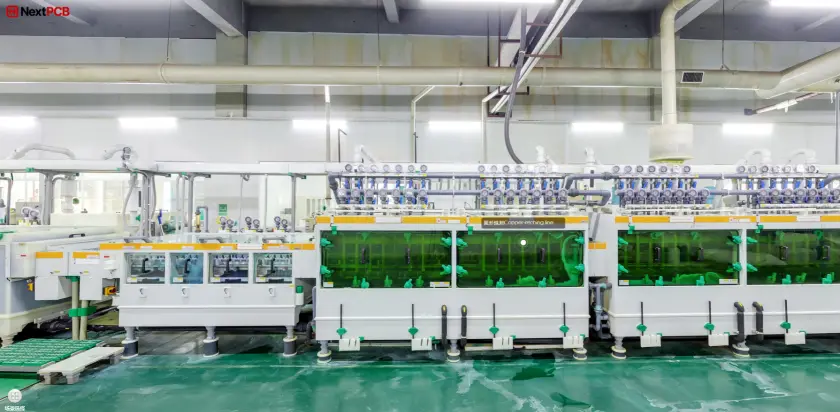
You don't have to take a factory's capability claims on faith. NextPCB makes this visible directly: see the PCB Factory VR Tour for a virtual walkthrough of the fabrication lines, or the PCB Assembly Factory Show for a look at the SMT equipment and process flow. When evaluating any manufacturer, ask whether they offer something equivalent — a factory tour, video walkthrough, or live production data — rather than relying only on marketing copy.
Certifications and Quality Standards to Check
Certifications aren't a formality — they indicate which quality management system a factory actually operates under, and which industries it's positioned to serve. When comparing manufacturers, ask for current certificates rather than relying on a logo on their website. As a reference point, NextPCB's facilities currently hold:
- IATF 16949 — the automotive industry's quality management standard, built on top of ISO 9001 with additional process controls.
- ISO 9001 — general quality management system certification.
- ISO 14001 — environmental management system certification.
- ISO 13485 — quality management for medical device manufacturing, relevant if your board is going into a regulated medical product.
- UL certification for both the U.S. and Canada, covering wiring and printed board safety listings.
- RoHS, REACH, and PFAS compliance documentation for hazardous substance restrictions in target markets.
One thing worth being direct about: NextPCB does not currently hold AS9100 (the aerospace-specific quality standard built on top of ISO 9001). If your project has an AS9100 requirement — common for aerospace and some defense-adjacent work — confirm this directly with any supplier before quoting, since certification status changes over time and shouldn't be assumed either way from a blog post. See the full certification and quality documentation page for current certificates.
Quick-Turn Prototypes vs. Volume Production
Most China-based fabricators offer both quick-turn prototyping and volume production, but the two have different priorities:
- Quick-turn prototyping optimizes for speed — getting a small number of boards (often 5–50 pieces) back quickly so you can validate a design before committing to a larger run. Turnarounds of 24–72 hours are common for standard specs.
- Volume production optimizes for consistency and cost per unit at scale, with more rigorous incoming material inspection and statistical process control across larger panel runs.
A manufacturer that only does one well isn't necessarily a bad choice — but if you expect to go from prototype to production with the same vendor, confirm they actually run both processes in-house rather than subcontracting one of the two stages.
Flex and HDI PCB Fabrication
Two board types are worth calling out separately because they carry tighter fabrication tolerances than standard rigid boards:
- Flex and rigid-flex PCBs use flexible substrate materials (typically polyimide) that require different lamination and etching handling than rigid FR4 boards. For design rules and material selection, see the Flex PCB capabilities page.
- HDI (High-Density Interconnect) PCBs use microvias and finer line/space geometries to pack more routing into a smaller board area — common in smartphones, wearables, and other space-constrained designs. See the microvia and HDI design guide for a breakdown of via types and design rules.
When comparing manufacturers for flex or HDI work specifically, ask about minimum trace/space, microvia aspect ratio limits, and whether laser drilling is done in-house — these are the areas where capability varies most between fabricators.
Fabrication + Assembly: The One-Stop (Turnkey) Option
Many teams sourcing circuit boards from China also need the boards assembled — components sourced, placed, and soldered. Splitting fabrication and assembly across two separate vendors means shipping bare boards internationally before they're even populated, adding a full freight cycle and a second point where boards can be damaged in transit.
Combining both stages under one vendor (commonly called turnkey) removes that extra shipping leg and puts quality accountability for the whole board in one place. This is a large enough topic that it has its own dedicated guide — see One-Stop PCB Manufacturing + Assembly (Turnkey): The Complete 2026 Guide for the full breakdown of full turnkey vs. partial turnkey vs. consignment, the step-by-step process, and what to check before choosing a turnkey partner.
Before You Order: Verify Your Files
Whichever manufacturer you choose, the highest-leverage step you can take before submitting an order is checking your Gerber files for manufacturability issues — footprint mismatches, clearance violations, and drill sizing problems are far cheaper to catch before production than after a board respin.
If you haven't settled on a DFM (design-for-manufacturability) tool yet, this comparison of the best free Gerber viewers in 2026 walks through ten options, including which ones offer real DFM analysis versus visual inspection only, and which are better suited to IP-sensitive projects that shouldn't be uploaded to a cloud service at all.
Shipping China-Made PCBs to the EU: 2026 Customs Changes
If you're ordering PCBs or PCBAs from China for delivery into an EU member state, a customs policy change took effect on July 1, 2026 that's worth knowing about before you place an order.
Previously, shipments valued at €150 or less were exempt from customs duty. As of July 1, 2026, that exemption has been removed: all shipments to EU destinations, regardless of value, are now subject to customs duty clearance. As a temporary measure (in effect until July 1, 2028), postal and IOSS shipments with an intrinsic value of €150 or less are charged a flat €3 per customs line item, where a "line item" groups goods sharing the same HS code, product description, and country of origin. Shipments above €150 are subject to standard customs duty rates. VAT rules are unchanged by this reform — VAT has applied to all EU imports since 2021.
A practical takeaway: consolidating smaller orders where possible can reduce the number of customs line items you're charged for, since duty is assessed per line rather than per shipment as a whole. This reform applies only to the 27 EU member states — the UK, Switzerland, Norway, and other non-EU European markets are unaffected.
For the full breakdown, including how customs lines are calculated and NextPCB's ongoing IOSS integration, see the official notice: Changes to EU Customs Policy Effective July 1st 2026. This is a fast-moving regulatory area — if you're planning EU-bound orders, check that notice directly for the current status rather than relying solely on a summary here.
How to Choose a China PCB Fabrication Partner
Bringing the sections above together, here's a practical checklist for evaluating a manufacturer:
- Can you verify their facility? Look for a factory tour, video walkthrough, or transparent equipment list rather than stock photography.
- Are their certifications current and relevant to your industry? Ask for documentation, and confirm any industry-specific requirement (AS9100, ISO 13485, etc.) directly — don't assume.
- Do they run fabrication and assembly in-house if you need both, or is one stage subcontracted?
- What's their DFM process? Is design review included standard, or a paid add-on?
- What are their quick-turn and volume production capabilities for your specific layer count, material, and trace/space requirements?
- How do they handle shipping and customs to your destination market, including any recent regulatory changes like the 2026 EU customs reform above?
Have a design ready to quote? Get an instant PCB quote, or if you need boards assembled as well, see PCB assembly quoting.
FAQ
What files are needed for PCB fabrication?
At minimum, a fabricator needs your Gerber files (one per copper, mask, and silkscreen layer), a drill file, and a stackup specification. For assembly, you'll also need a BOM and a centroid/pick-and-place file. See the file requirements guide for a full breakdown.
How long does PCB fabrication take?
Quick-turn prototype orders for standard specifications commonly ship within 24–72 hours; volume production runs and boards with advanced specs (fine line/space, high layer counts, unusual materials) take longer. Confirm current lead times for your specific board and quantity when requesting a quote, since capacity and turnaround vary by order volume and time of year.
Is PCB fabrication from China AS9100 certified?
It depends on the manufacturer — AS9100 is not a universal certification across Chinese PCB fabricators. NextPCB, for example, holds IATF 16949, ISO 9001, ISO 14001, ISO 13485, and UL certification, but does not currently hold AS9100. If your project requires AS9100 specifically, confirm certification status directly with any supplier before ordering.
Will I pay customs duty on PCBs shipped from China to the EU?
As of July 1, 2026, yes — the previous €150 duty-free exemption for EU imports was removed. Low-value postal and IOSS shipments (€150 or under) are now subject to a temporary €3 per customs line item until July 1, 2028; shipments above €150 are subject to standard duty rates. This applies only to EU member states. See the full customs reform notice for details.
Can I fabricate a PCB at home instead of outsourcing to China?
For very simple single- or double-layer boards, hobbyist etching kits exist, but home fabrication generally can't match the plating quality, drill precision, or layer registration of a commercial fabricator — and it becomes impractical past two layers or for anything requiring plated through-holes. For anything beyond a basic prototype, outsourcing to a fabricator is almost always more reliable and, once you factor in materials and time, often cheaper per board too.