
 NextPCB Capabilities
Printed Circuit Boards
NextPCB Capabilities
Printed Circuit Boards
 PCB Assembly
 Layer Buildup
 SMD-Stencils
 PCB Design-Aid & Layout
 Mechanics
 Quality
 Drills & Throughplating
 Factory & Certificate
 PCB Assembly Factory Show
Certificate
PCB Assembly Factory Show
Certificate
Support Team
Feedback:
support@nextpcb.com


At low signal frequencies, trace parasitics have a negligible effect on circuit behavior. Once signal frequencies reach the hundreds of MHz to GHz range, however, traces must be treated as transmission lines rather than simple conductors. At that point, the characteristic impedance of each trace determines whether signal energy travels cleanly to its destination or gets partially reflected back, causing distortion.
Characteristic impedance is not governed by trace width alone. It is the combined result of four interdependent parameters:
Each of these parameters belongs to a different stage of the PCB development process. They must be determined in sequence and cannot be adjusted arbitrarily once routing begins.
The following table lists common interface impedance requirements for reference. Always verify against the latest version of the relevant specification before finalizing your design targets.
| Interface | Impedance Target | Trace Type |
|---|---|---|
| USB 3.0 / 3.1 | 90Ω ±10% | Differential pair |
| PCIe Gen1–5 | 85Ω ±10% | Differential pair |
| DDR4 / DDR5 data lines | 40–50Ω | Single-ended |
| General RF / single-ended | 50Ω ±10% | Single-ended |
| HDMI | 100Ω ±15% | Differential pair |
Before getting into the specifics, it helps to understand where impedance control sits within the overall PCB development timeline. The complete chain, from specification input to manufacturing delivery, is as follows:
1. Interface Specification Review
   └─ Identify which nets require impedance control, along with target values and tolerances

2. Stackup Definition
   └─ Confirm materials, thicknesses, and copper weights with the manufacturer → freeze the stackup

3. Impedance Calculation (SI9000 or equivalent tool)
   └─ Use impedance targeting to back-calculate trace widths and spacings for each layer

4. Fabrication Feedback Loop - ! Frequently skipped
   └─ Submit SI9000 parameters to the manufacturer → manufacturer back-calculates widths
      using actual lamination data → returns confirmed design values
   └─ For tight-tolerance projects (±5%), this step is mandatory and cannot be omitted

5. Allegro Constraint Entry
   └─ Enter manufacturer-confirmed trace widths into Constraint Manager and assign to nets

6. Routing Execution
   └─ Route with constraint-driven tools; maintain reference plane continuity and return path integrity

7. Manufacturing Delivery and Impedance Verification
   └─ Submit impedance spec document + coupon locations → explicitly request TDR testing from the manufacturer
Each step in this chain depends on the one before it. If the stackup changes, all impedance calculations must be rerun. If constraints are modified, every already-routed net affected by the change needs re-verification. Step 4 — the fabrication feedback loop — is the single most commonly skipped step in practice. Yet it marks the true boundary between rigorous and approximate impedance control: SI9000 results from the design side are an initial estimate; the manufacturer's back-calculation based on actual lamination thickness is the authoritative design input.
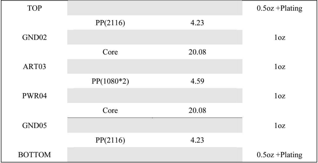
Fig 1: Typical 6-layer 1.6mm PCB stackup design example
Using the 6-layer, 1.6 mm PCB shown in Figure 1 as an example, the stackup structure is as follows:
| Layer | Material | Thickness (mil) | Copper Weight |
|---|---|---|---|
| TOP | — | — | 0.5 oz + plating |
| Dielectric | PP (2116) | 4.23 | — |
| GND02 | — | — | 1 oz |
| Dielectric | Core | 20.08 | — |
| ART03 | — | — | 1 oz |
| Dielectric | PP (1080×2) | 4.59 | — |
| PWR04 | — | — | 1 oz |
| Dielectric | Core | 20.08 | — |
| GND05 | — | — | 1 oz |
| Dielectric | PP (2116) | 4.23 | — |
| BOTTOM | — | — | 0.5 oz + plating |
Several points in the stackup design phase require particular attention:
Copper thickness must be confirmed with the manufacturer. The outer layers (TOP and BOTTOM) are listed as 0.5 oz base copper plus plating. After electroplating, total copper thickness is roughly 1 oz (35 μm), but the exact value depends on the manufacturer's plating process and typically carries a tolerance of ±10%. Copper thickness directly affects the trapezoidal cross-section of the trace, which in turn affects effective trace width and the impedance calculation. Always use the manufacturer-confirmed copper thickness as the T1 input in SI9000, not the nominal value.
Er is frequency-dependent. FR4 laminate has a nominal Er of approximately 4.2–4.6 at 1 MHz, but this drops to roughly 3.7–4.0 in the GHz range, with the exact value varying by material grade and frequency. The Er value used in SI9000 should correspond to the operating frequency of the signals being routed. Request measured Er data at the relevant frequency from the laminate supplier rather than using low-frequency datasheet values.
The stackup must not be changed once frozen. The stackup is the foundational input for all impedance calculations. Any subsequent change — for example, substituting a 2116 prepreg with a 1080 — invalidates every previously calculated trace width and spacing, requiring a full recalculation. The cost of making this change late in the project is significant. Confirm and freeze the stackup with the manufacturer before layout is complete.
Inner signal layers reference both adjacent planes. ART03 has GND02 as its upper reference layer (separated by a 20.08 mil Core) and PWR04 as its lower reference layer (separated by a 4.59 mil PP prepreg). Inner layer routing uses a Stripline model, and characteristic impedance is influenced by both reference layers simultaneously. SI9000's Symmetric Stripline or Asymmetric Stripline models account for both reference distances. Using only the nearer of the two planes for the calculation is not sufficient.
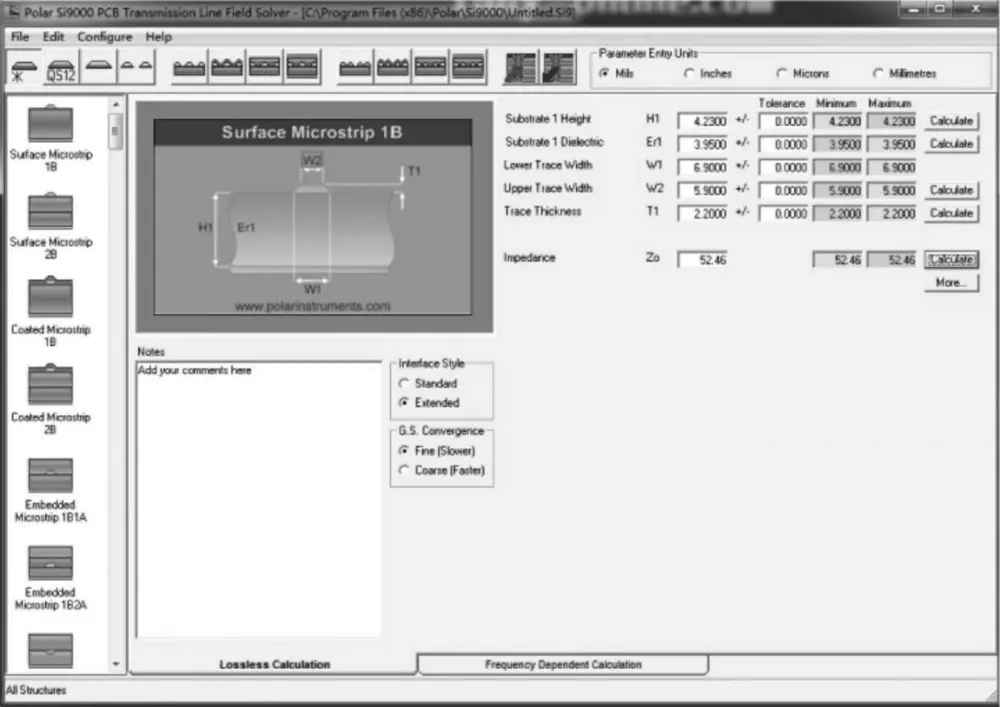
For single-ended 50Ω traces on the TOP or BOTTOM layer, the appropriate SI9000 model is Surface Microstrip 1B (Figure 2). This model applies to traces on the surface of a dielectric with a single reference plane beneath — the standard outer-layer configuration.
Enter the stackup parameters into SI9000 as follows:
| Parameter | Symbol | Value (mil) |
|---|---|---|
| Dielectric height (PP 2116) | H1 | 4.23 |
| Relative permittivity | Er1 | 3.95 |
| Trace width at base | W1 | 6.9 |
| Trace width at top | W2 | 5.9 |
| Copper thickness | T1 | 2.2 |
Calculated result: Zo = 52.46Ω, which falls within the ±10% tolerance band of 45–55Ω for a 50Ω target.
Understanding W1 and W2: The etching process produces a trapezoidal cross-section rather than a rectangle. The base of the trace (W1) is wider than the top (W2), with the difference determined by the etch factor. The etch factor is available from the manufacturer on request. The width dimension annotated in the layout tool and the relationship of that dimension to W1 or W2 depends on the manufacturer's internal etching model: some manufacturers use the base width (W1) as the reference, others use the top width (W2) or a mid-width value, with etch compensation applied internally. Since the design engineer typically cannot determine which convention a given manufacturer uses, this should be explicitly clarified during the stackup confirmation stage to ensure both parties are working from the same reference point.
Solder mask effect on impedance: The Surface Microstrip model assumes the trace surface is either bare or that the solder mask effect has been modeled separately. In practice, outer-layer traces are covered by solder mask, whose dielectric properties reduce actual impedance by approximately 1–3Ω. For projects with tight tolerances (±5% or less), the solder mask parameters (Solder Mask Height and Solder Mask Er) should be explicitly entered in SI9000 rather than omitted.
Use impedance targeting (back-calculation) to obtain the trace width: Rather than manually entering multiple width values and iterating toward a result, fix the target impedance (50Ω) in SI9000 and use the Calculate function to back-calculate W1. Submit this initial value to the manufacturer, who will re-verify it against actual lamination data and return a confirmed design width. The two together form a complete and defensible design input.
| Send Your Allegro Stackup to NextPCB for Manufacturer Confirmation |
After defining your impedance constraints in Allegro's Constraint Manager, the next step is manufacturer confirmation. Submit your stackup requirements to NextPCB — we'll verify Er, trace width, and prepreg combination, then return a signed stackup drawing within 24 hours.
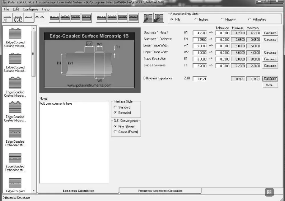
Differential pair impedance control introduces an additional variable: the coupling between the two traces. The appropriate SI9000 model is Edge-Coupled Surface Microstrip 1B (Figure 3).
Input parameters:
| Parameter | Symbol | Value (mil) |
|---|---|---|
| Dielectric height | H1 | 4.23 |
| Relative permittivity | Er1 | 3.95 |
| Trace width at base | W1 | 5.0 |
| Trace width at top | W2 | 4.0 |
| Edge-to-edge spacing | S1 | 8.0 |
| Copper thickness | T1 | 2.2 |
Calculated result: Zdiff = 109.21Ω. The acceptable range for a 100Ω ±10% target is 90–110Ω, placing this result at the upper edge of the tolerance band.
Differential impedance and odd-mode impedance: When SI9000 calculates differential impedance, it first solves for odd-mode impedance (Zodd) and then derives the differential result using the relationship Zdiff ≈ 2 × Zodd. Even-mode impedance (Zeven) describes the common-mode signal path; when both traces in a differential pair are routed symmetrically and carry signals of opposite polarity, even-mode effects cancel out. Day-to-day impedance control therefore focuses on odd-mode and differential impedance. Understanding this relationship enables correct interpretation of SI9000 output pages and supports accurate communication with SI simulation engineers.
Manufacturing tolerance risk: Differential impedance is more sensitive to changes in spacing (S1) and copper thickness (T1) than single-ended impedance. Based on the parameters in this example, reducing S1 by 1 mil causes Zdiff to drop by approximately 3–5Ω; a 10% increase in copper thickness affects Zdiff by approximately 1–2Ω. When multiple process variations shift in the same direction simultaneously, the actual impedance can exceed the tolerance window. Design targets should therefore be placed at the center of the tolerance range rather than at its edges, preserving margin for process variation. For a 100Ω ±10% requirement, aim for a calculated result in the 98–102Ω range rather than landing at 90Ω or 110Ω.
Definition of S1: In SI9000, S1 is the edge-to-edge spacing between the two traces of the differential pair. The Gap parameter in Allegro's differential pair constraint system also uses an edge-to-edge definition. Once this consistency is confirmed, S1 can be entered directly as the constraint value without any unit conversion.
Navigate to Setup → Constraints → Constraint Manager (or press the shortcut key CM). Constraint Manager is the central hub for all constraint types in Allegro: physical rules, spacing rules, and differential pair rules are all managed here.
In the Physical domain:
SE_50OHM_TOP.DIFF_100OHM_TOP for differential pairs, applying the same width-range logic.In the Net view, locate the differential net pair (e.g., USB_DP / USB_DM) and define it as a Differential Pair. A complete differential pair constraint set must include more than just spacing. The required parameters are:
Configuring only the Primary Gap while leaving phase and length-matching constraints undefined is the most common form of incomplete differential pair setup. DRC will pass nets that do not actually meet the interface specification.
Navigate to Setup → Cross-section and enter each layer's material, thickness, and copper weight to match the confirmed stackup design. This data feeds Allegro's internal impedance estimation feature. Keeping it consistent with the SI9000 input parameters allows both tools to serve as cross-checks on each other.
Mistake 1: Determining trace width during the routing phase. Impedance trace widths must be established after the stackup is confirmed and before floorplanning begins, then written into the design rules as constraints. Discovering during routing that impedance-required widths do not fit the existing component placement typically leads to significant rework.
Mistake 2: Routing signal traces across reference plane splits. Impedance calculations assume the reference plane is a continuous, uninterrupted copper fill. When a signal trace crosses a split in a power plane, the reference is locally absent, causing the actual impedance to deviate from the modeled value and introducing substantial ground return noise. Enable the anti-pad and plane-crossing DRC checks in Allegro, or plan the plane split locations during floorplanning so that they do not intersect critical signal paths.
Mistake 3: Neglecting return path continuity at layer transitions. In high-speed design, signal return path continuity is at least as critical as impedance itself — and is more frequently overlooked. Every time a signal transitions to a different layer through a via, its return current must find a continuous path on the reference plane. If the reference plane changes at that layer transition (for example, from a GND plane to a PWR plane), the return path is interrupted. This creates a local impedance discontinuity and is a common source of EMI problems. The correct solution is to place stitching vias adjacent to the signal via, locally connecting the two reference planes and restoring return path continuity.
Mistake 4: Applying outer-layer Microstrip widths to inner signal layers. Stripline and Microstrip have different field distributions. For a given dielectric height, inner-layer Stripline traces typically require a narrower width than outer-layer Microstrip traces to achieve the same impedance. Both must be modeled separately in SI9000 using their respective model types. Sharing a single trace width dataset between outer and inner layers is a systematic error.
Mistake 5: Not addressing impedance discontinuities at vias. Every via in a high-speed signal path introduces parasitic inductance (via inductance) and parasitic capacitance (via capacitance), creating a localized impedance discontinuity. For signals above approximately 3 GHz, back drilling should be considered to reduce via stub length, or blind and buried vias should be used to minimize via height.
Mistake 6: Omitting the impedance specification document when submitting for fabrication. Some engineers embed the correct trace width in the Gerber files but do not separately communicate impedance control requirements to the manufacturer. Without an explicit instruction, the manufacturer will produce the board to the geometric dimensions only and will not perform impedance testing. The impedance specification document — listing which layers, which nets, target values, and tolerances — must accompany the fabrication package.
When signal operating frequencies exceed 5 GHz, standard FR4 laminate becomes a limiting factor due to its relatively high dielectric loss (Df ≈ 0.02). Impedance control is still achievable, but signal attenuation along the trace becomes the dominant constraint. Low-loss laminates should be considered. Common options include:
Low-loss laminates have Er values that differ from FR4. SI9000 models for these materials must use the laminate's actual Er and copper foil roughness (copper foil roughness) parameters. Using FR4 defaults in place of the actual material data produces results with no engineering validity.
Once routing is complete and Gerber files have been generated, three additional items must be provided to the manufacturer to ensure impedance control requirements are actually executed:
This point deserves emphasis: TDR testing is not performed by default. Impedance testing using a time-domain reflectometer is only carried out when the customer explicitly requests it and the associated cost is agreed upon. Some engineers assume that annotating a target impedance value on the fab drawing is sufficient to trigger testing; in practice, the manufacturer will produce the board to the specified line widths and will not independently verify impedance unless instructed to do so. For projects with quality record requirements — telecommunications equipment, medical electronics, automotive electronics, and similar — the TDR test report must be specified as a formal deliverable in the procurement document.
Many PCB manufacturers with controlled-impedance capability (including NextPCB) support submission of an impedance specification document and coupon location data at the time of order, and will proactively review stackup parameters during the engineering confirmation stage. A third-party TDR test report can be provided upon explicit customer request.
Precision impedance control requires more than just a good layout—it needs a manufacturing partner who understands signal integrity. At NextPCB, we provide expert stackup consultation, ±5% impedance tolerance management, and verified TDR testing reports for your advanced PCB projects.
Q1: My SI9000 calculation result and the manufacturer's TDR test report are off by a few ohms. What typically causes this?
The two most common causes are these. First, PP prepreg compresses during lamination, so the actual cured thickness is less than the nominal value — typically 5–10% thinner — which directly reduces the dielectric height H1. Second, plated copper thickness carries its own tolerance; if the actual copper weight differs from the T1 value used in SI9000, the trapezoidal cross-section geometry shifts, and impedance shifts with it. Once you have the manufacturer's measured stackup report, re-enter the actual parameters into SI9000. In most cases, the two results align within ±2Ω. A discrepancy larger than ±5Ω warrants a closer look at whether the etch compensation factor is consistent between both models.
Q2: Allegro's DRC passed with no violations. Does that mean impedance control is complete?
DRC only verifies that trace geometry satisfies the constraint rules — line width, spacing, and so on. It cannot confirm whether the physical impedance value is correct. Characteristic impedance is an electrical property determined jointly by trace geometry and stackup material; Allegro has no way to guarantee it automatically during routing. If your constraint rules are consistent with the SI9000 calculation results, and the reference planes are continuous, then impedance is under control at the design level. Verification at the manufacturing level requires TDR testing by the fabricator.
Q3: Does the edge-to-edge spacing of a differential pair need to remain constant through serpentine tuning sections?
Yes. The edge-to-edge spacing (S1) must remain consistent along the entire routed path, including through serpentine sections and at corners. Any variation causes local differential impedance to deviate from the designed value and degrades the common-mode rejection ratio (CMRR). Allegro's Interactive Differential Pair Routing tool, when constraints are properly configured, maintains the specified spacing automatically through tuning sections. Manual adjustments that violate the spacing constraint will be flagged by DRC.
Q4: Do inner-layer traces require the same width as outer-layer traces to achieve the same impedance?
No. Outer-layer traces have a single reference plane below and are modeled using Microstrip. Inner-layer traces are sandwiched between two reference planes and are modeled using Stripline — either Symmetric or Asymmetric depending on whether the dielectric heights above and below are equal. For the same dielectric height, inner-layer Stripline traces typically need a narrower width than outer-layer Microstrip traces to achieve the same target impedance. Each configuration must be modeled separately in SI9000 using the correct model type. Applying a single width dataset to both outer and inner layers is a systematic error.
Q5: The manufacturer's confirmed stackup differs from what I used for impedance calculations. Do I need to re-route the board?
It depends on the magnitude of the deviation relative to the impedance tolerance. Start by entering the manufacturer's actual stackup parameters into SI9000 and back-calculating the required trace width. If that width differs from the current routed width by no more than 0.5 mil, and the resulting impedance still falls within the tolerance band, re-routing is generally not required — though the manufacturer should confirm this through the TDR test report. If the deviation pushes impedance outside the tolerance window, you must negotiate a stackup adjustment with the manufacturer (changing the PP specification or adjusting lamination thickness), recalculate trace widths against the new stackup, and update the routing accordingly. This is precisely why the stackup should be confirmed and frozen before routing starts rather than after.
Still, need help? Contact Us: support@nextpcb.com
Need a PCB or PCBA quote? Quote now


 Surface

