

 NextPCB Capabilities
 PCB Assembly
 Layer Buildup
 SMD-Stencils
 PCB Design-Aid & Layout
 Mechanics
 Surface
 Quality
 Drills & Throughplating
 Factory & Certificate


Introduction
The fierce competition in modern electronics manufacturing centers on miniaturization and extreme performance breakthroughs. When product designs reach industry-recognized limits, such as requiring the installation of almost invisible 01005/0402 passive components or integrating ultra-high-density 0.25mm Pitch BGA/QFN packages, standard Printed Circuit Board Assembly (PCBA) providers often fall short.
Surface Mount Technology (SMT) is the core engine of the PCBA process; its precision and stability directly determine the reliability and yield of the final product. At NextPCB, we understand that profound expertise in cutting-edge SMT processes is the fundamental guarantee for providing comprehensive PCBA solutions for global clients, spanning high-standard applications in Automotive (IATF 16949) and Medical (ISO 13485) sectors.
This article will delve into how NextPCB transforms these complex SMT challenges into core strengths of our High-Density Assembly Capability through extreme process control, massive scale, and stringent quality systems, delivering unparalleled reliability for your projects.
I. New Frontiers of Miniaturization: The Challenges of 01005 and Ultra-Fine Pitch
The rapid development of the Internet of Things (IoT), wearables, and 5G modules has pushed electronic products to unprecedented levels of component density. This necessitates SMT assembly capabilities that can address two critical technical bottlenecks: the absolute size of components and the pitch between them.
> Recommend reading: PCBs Power Electronic Devices: Wearables, IoT & Smart Homes
1.1 Conquering the Physical Limits of 01005 Components
The 01005 component, measuring just 0.4 mm x 0.2 mm, equivalent to the metric 0402 package, is smaller than a grain of salt and represents one of the most precise passive components used in the industry today. The manufacturing challenges associated with this size go far beyond simply placing the part on the board:
-
Solder Paste Printing: The pads for 01005 components are typically only 200–220 µm in length and width. Solder paste deposit consistency is paramount, as even the slightest deviation can cause soldering defects like "tombstoning" or opens.
-
Placement Accuracy: The extremely low weight (approximately 0.04 mg) and minuscule dimensions of the component demand pick-and-place machines with sub-micron accuracy and stable vacuum suction.
-
Inspection Difficulty: The 01005 package is nearly impossible to inspect effectively using the naked eye or standard optical inspection equipment. > PCB/PCBA Test Methods by Category
NextPCB intervenes early in the design stage to ensure pad geometries and clearances (less than 160 µm) meet high-yield requirements, combining this with advanced printing technology to stably assemble 01005/0402 passives.
1.2 0.25mm BGA: The Process Barrier of High-Density Interconnect
Ball Grid Array packages, with solder joints located beneath the component body, are indispensable for high-density PCB designs. While the industry generally considers a 0.5mm pitch to be a significant challenge, NextPCB confirms its ability to reliably handle components with pitches as low as 0.25mm pitch BGA/QFN.
This ultra-fine pitch BGA assembly requires manufacturers to have extreme control over solder paste printing and reflow profiles, as any slight variation in paste volume or temperature can lead to shorts or open circuits.
II. NextPCB's Precision SMT Manufacturing Roadmap
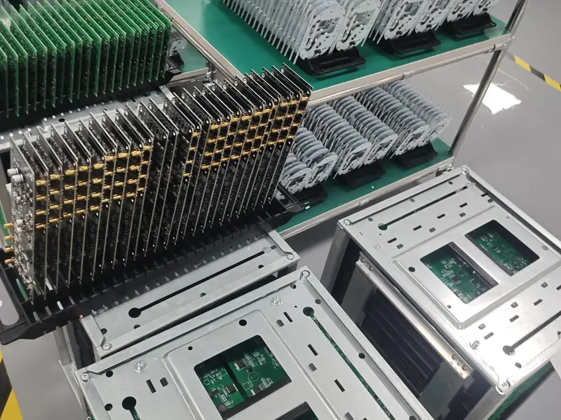
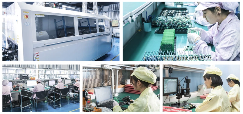
Achieving these cutting-edge capabilities relies on a systematic, traceable manufacturing process supported by NextPCB's 36 automated Siemens SMT production lines.
> Assembly Factory Show - NextPCB
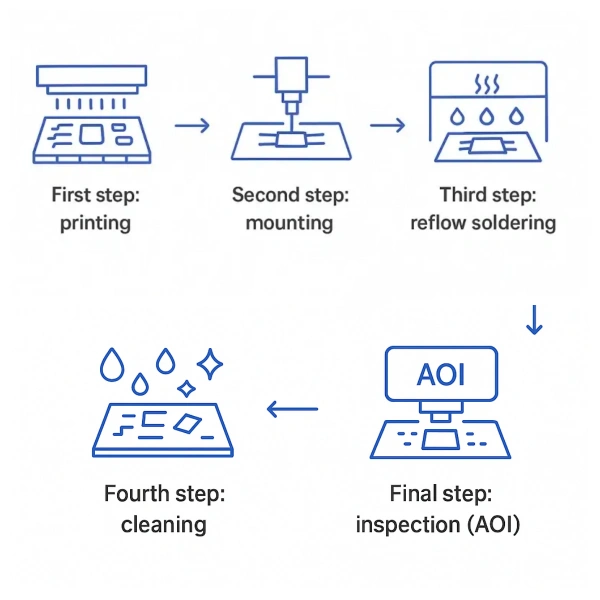
2.1 Ultra-Precise Solder Paste Control
Solder paste printing is the foundation of successful SMT assembly. To ensure precise and consistent solder paste volume on both 0.25mm BGA and 01005 pads, NextPCB utilizes key technologies:
-
Laser-Cut Stencils: We use stencils that are laser-cut and electro-polished, which ensures smooth, complete release of solder paste from extremely small apertures, preventing clogging and slumping.
-
Fine Particle Solder Paste: For 0.25mm fine pitch and 01005 pads, it is mandatory to use Type 3 or finer no-clean solder paste with reduced particle size to guarantee printing accuracy and excellent wetting during reflow.
2.2 Sub-Micron Component Placement and Mixed Assembly Compatibility
NextPCB's automated production lines achieve component placement with extremely high speed and accuracy, boasting a daily assembly capacity of over 95 million solder joints.
In high-density layouts, machines rely on Fiducial Marks to provide accurate alignment references. For high-density PCB designers, our ability to manage minimum clearances between components (e.g., standard 0.2 mm clearance, or even tighter 0.1 mm clearance for dense designs) is critical for ensuring project yield.
Furthermore, NextPCB offers full Mixed Technology Assembly (SMT & THT). This ensures that designs requiring Through-Hole (PTH) components, such as large connectors or high-power thermal devices, can be supported with reflow, as well as wave or manual soldering, ensuring both functionality and reliability.
III. The Quality Mandate for High-Reliability PCBA: Inspection and Certification
The inherent risks of high-density SMT manufacturing must be eliminated through multi-layered and mandatory quality inspection.
3.1 Mandatory X-Ray Verification and Multi-Level Inspection
To address the issue of BGA solder joints being invisible beneath the component, NextPCB strictly enforces mandatory X-Ray verification for all BGA placements. X-Ray inspection is the only non-destructive method capable of verifying BGA solder ball formation, voiding rates, and accurate pad alignment.
Our multi-tiered inspection system includes:
-
SPI (Solder Paste Inspection): Three-dimensional solder paste volume inspection immediately after printing.
-
AOI (Automated Optical Inspection): High-speed checking of component alignment and polarity after placement.
-
FCT (Functional Testing): We provide free Functional Testing services, which significantly reduces the manufacturing risk and debugging costs associated with high-difficulty SMT.
3.2 International Certification and Workmanship Standards
Our cutting-edge SMT capabilities are not based on singular attempts but are built upon a repeatable, high-standard quality system. NextPCB's assembly process adheres to the IPC-A-610 Class 2 workmanship standard, and IPC Class 3 assembly is available upon request for clients with the most critical requirements. > IPC Class 2 vs 3: The Differences in PCB IPC Standards
Crucially, NextPCB holds IATF 16949:2016 (Automotive Electronics) and ISO 13485:2016 (Medical Devices) certifications. This means our processes can handle high-difficulty designs like 01005 and 0.25mm BGA while simultaneously meeting the highest requirements for reliability, traceability, and long-term stable operation in the automotive and medical fields.
IV. Your PCBA Partner: Scale and Speed
NextPCB's SMT technical prowess is integrated with our scaled services, designed to provide a seamless and rapid manufacturing experience.
4.1 Rapid Delivery and Engineering Support
NextPCB is committed to applying high-difficulty technology to rapid delivery. We offer quick turnaround capabilities, such as 24-hour assembly for Quick Turn Turnkey PCBA service, contingent upon all components being ready.
Recognizing the high risk associated with high-density SMT designs, we provide a free DFM/DFA review service. Our DFM/DFA team intervenes early in the design stage to help you optimize pad design and component spacing, transforming technical risk warnings into opportunities for NextPCB services. We are currently offering a limited-time promotional discount to help you further reduce your PCBA costs.
> Recommend reading: PCB Assembly Cost - Affecting Factors and Way to Save Money
4.2 Comprehensive Supply Chain and Value-Added Services
As a full-service PCBA provider, NextPCB offers a range of value-added services, including IC Programming, Conformal Coating, and Laser Coding. Through NextPCB HQ Online Component Sourcing services, you can achieve a true end-to-end Turnkey solution, guaranteed by a single, reliable source with advanced SMT capabilities, from design to finished goods shipment.
Conclusion
NextPCB's stable assembly capability for 01005 components and 0.25mm BGA, coupled with its adherence to mandatory X-Ray inspection, is the best technical proof of our overall PCBA service excellence.
When facing your next-generation high-density design challenges, choosing NextPCB means selecting not just advanced equipment but also a manufacturing process certified by the highest standards in the automotive and medical industries. We offer IPC Class 3 quality standard assembly, 0.25mm fine pitch capability, and in-depth DFM/DFA review to ensure your project achieves maximum reliability.
Visit our NextPCB High-Density Assembly Capability core page today to take advantage of instant online quoting and ordering, and Get $200 Off to kickstart your In-house Turnkey PCB Assembly project!


