Table of Contents
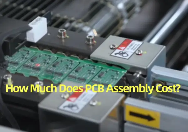
How much does PCB Assembly Cost?
PCB assembly costs include various expenses such as labor, turnaround time, technology, PCB quality, and parts packaging. specialized pcb assembly cost calculator tools can estimate manufacturing expenses including operational overhead. The unit price per printed circuit boards depends on production volume and board type. PCB types include 5G PCBs, High-Density Interconnect PCB (HDI), Flexible PCB, etc.
Key PCB manufacturing cost is affected by various factors, which are as follows:
Labor Cost
The labor cost is one of the impacting factors in the price of PCB manufacturing. Geographical location significantly impacts labor expenses. Besides, the manufacturing of PCB includes a skilled human workforce and automated machines. Some overseas manufacturing could increase the cost because of shipping delays and communication barriers.
Turnaround Time
The expected turnaround time is one of the common factors that affect the assembly cost of PCB. It can call the turnaround time required for completing the manufacturing process and satisfying the request of the customers. Expedited production schedules can increase pcb assembly prices by up to 33%. Shorter leadtime requires prioritized resources.
Quantity
Higher volumes will reduce per-unit price through economies of scale. Bulk orders lower upfront costs like programming setup for surface mount technology (SMT). In this process, the unit prices of each PCB drop significantly helping firms save money in the long run. It happens as the firm can control various factors that affect the assembly cost, like startup programming and cost and initial unit cost.
Technology
PCB assembly uses two primary methods of technology: Through-Hole Technology (THT) and Surface Mount Technology (SMT). In the SMT process, the setup cost is lower than heavy automation. However, SMT is required in through-hole drilling.
Parts Packaging
Some of the sensitive components require X-ray inspection to prevent shorts . This increase the labor cost as the proper assembly is the goal. Special handling for complex designs like BGAs increases labor time.
PCB Size & Panel Utilization
Another crucial factor that affects the cost of PCB includes the size of PCB and the panel utilization. These two elements dictate material waste. (Learn How to Layout a PCB Panel for Much Less Cash)
The number of circuits can determine the board size required. On the other hand, the component's amount of space can also affect the price. Thus, the dimensions of the PCB design determine the overall costs of PCB.
Material Choice
The material used in the PCB board affects the cost of the assembly process. For example, standard FR4 laminate suits most applications, but high-frequency designs demand pricier materials like polyimide for aerospace systems. Thus, the materials used in microwaves or aerospace and fuel industries can cost more than that of handheld devices.
Number of Layers
The number of layers involved in PCB is one of the other factors that determine the price of the PCB. Multilayer board assemblies (especially 10+ layers) require precise drilling and lamination. Accordingly, layerboard count exponentially increases defect risks and processing steps.
The two-layered PCB board costs lesser compared to 3 and higher-layer boards. Since the thick layer board requires more work in manufacturing. Besides, the pricing issue is also affected by board size and the materials used. Besides, assembling the multi-layer board requires various steps, and there is a high chance of defects. Thus to counter this issue, PCB makers provide extra efforts. However, it will ultimately increase the cost of the assembly.
Size of Hole
The hole size of the PCB board is also one factor that can affect the cost of PCB production. The required number of holes in the board and the thickness of layers and material types to be drilled also determine the price. Micro-vias (<0.15mm) need laser drilling and specialized tools. Double sides boards with blind vias add processing time.
For example, the PCB board with ten or more layers requires more time to drill. Also, if the materials were strong, the drilling process would have been more complex, impacting the price of the PCB. The super thin hole requires a unique tool to produce. This ultimately increases the price of the production.
PCB Finish
The cost of finishing is also the factor affecting the PCB's cost. The finishes that have higher grade offers a longer shield life. Higher-grade finishes like ENIG (Electroless Nickel Immersion Gold) or Immersion Silver (IAG) extend lifespan but raise costs vs standard HASL finish.
Top 5 PCB Surface Finishes Explained: ENIG, HASL, OSP, ISN, and IAG with Solderability Benefits
|
Surface Finish
|
Solderability
|
Wire Bondable
|
Surface Flatness
|
Cost
|
Storage Life
|
Additional Key Features
|
|
ENIG (Electroless Nickel Immersion Gold)
|
Excellent
|
Yes (AI-compatible)
|
Excellent
|
High
|
Long
|
Suitable for fine-pitch components, high reliability
|
|
HASL (Hot Air Solder Leveling)
|
Good
|
No
|
Poor (especially for BGA)
|
Low
|
Medium
|
Low cost, not ideal for HDI or fine-pitch components
|
|
OSP (Organic Solderability Preservative)
|
Good
|
No
|
Good
|
Very Low
|
Short
|
Environmentally friendly, RoHS compliant, short shelf life
|
|
ISn (Immersion Tin)
|
Good
|
No
|
Good
|
Medium
|
Medium
|
Flat surface, not suitable for multiple reflow cycles
|
|
IAg (Immersion Silver)
|
Very Good
|
Yes (AI-compatible)
|
Very Good
|
Medium-High
|
Medium
|
Sensitive to handling and tarnish, good for fine-pitch
|
Recommend Reading: HASL vs ENIG: An Ultimate Guide on Surface Finish
How To Save Money On PCB Assembly?
PCB Design Optimization
Proper designing of PCB helps in reducing the cost of PCB assembly. Simplify complex designs by:
- 1. Reducing layer count
- 2. Standardizing surface finish types
- 3. Optimizing board size and panel utilization
When manufacturing the PCB, you can redesign each of the elements mentioned above to reduce the cost of the PCB.
Comprehensive Bill of Materials(BOM)
Accurate BOM lists prevent delays. Include:
- Alternate part number options
- Reference designator mapping
- Footprint specifications
It should create the bill of materials(BOM) to list all the components in the PCB board. The PCB design checklist can determine all the required BOM, including footprints, parts numbers, reference designators, and assemblers. BOM should also include the alternative components or parts for each used component on the board.
Order Volume & Leadtime
Large orders volume is critical for price determinations. According to the concept of economy of scale, the higher the order volume, the less the unit price. Therefore, you should select the manufacturer based on your order size and the manufacturer's turnaround time.
Balance turnaround time needs with production flexibility using pcb assembly cost calculators.
Inspection & Testing
The cost reduction should not compromise the quality of the PCB board. Thus the testing and inspection of the product is a must before sending the product to market. The temperature of the traces on board requires proper monitoring. It could be in both internal and external layers. Proper inspection and ensuring the circuit is adaptive to changing temperatures can minimize the long-term risk.
Why is PCB Assembly so Expensive?
The cost of PCB design and manufacturing is determined by various factors like intricacy of design, elements types, and project effectiveness. In addition, the complexity and nature of the circuit also determine the assembly cost of PCB. In contrast, the final price is affected by the quality of the PCB design.
PCB assembly is expensive due to leadless components and precise pitching. It is because it requires testing methodologies, including a unique assembly process. The cost of fundamental ingredients leads to the higher cost of the PCB assembly. The production and assembly of printed circuit boards (PCBs) to meet the needs of various sectors is done at a high technology level. PCB assembly expenses, therefore, depend on factors directly related to companies, products, and assembly methods.
Besides, the PCB assembly option also factors in the cost of the PCB in two ways:
- 1. Costlier material
- 2. As a result of production irregularities, every assembly procedure requires some retesting.
- 3. The assembly method also impacts the performance and fabrication cost of PCB.
SMT vs THT Cost Analysis
In terms of cost-efficiency, SMT clearly outperforms THT. The elimination of drilling, the use of automated soldering, and the smaller size of SMD components collectively contribute to a significant reduction in manufacturing and assembly costs. SMT is highly suitable for high-volume, high-density, and automated PCB production.
On the other hand, THT involves higher costs due to manual labor, drilling requirements, and slower production rates. While THT may still be favored in certain applications—such as prototyping or mechanically stressed environments—it is generally less cost-effective than SMT in modern electronics manufacturing.
SMT vs. THT: Cost-Focused Comparison Table
|
Comparison Aspect
|
SMT (Surface Mount Technology)
|
THT (Through-Hole Technology)
|
|
Overall Cost
|
Lower overall cost
|
Higher overall cost
|
|
Drilling Cost
|
No drilling required (components mounted directly on PCB surface)
|
Requires precise hole drilling for every lead, adding machining cost
|
|
Assembly Method
|
Fully automated soldering reduces labor and improves efficiency
|
Manual soldering increases labor cost and time
|
|
Material Usage
|
Smaller SMD components use less material
|
Larger components and additional copper layer area increase cost
|
|
Production Speed
|
Faster automated placement lowers time-per-unit
|
Slower manual placement increases production time and cost
|
|
Design Impact on Cost
|
Supports compact layout, reducing board size and overall BOM cost
|
Bulky layout may increase PCB size and layer count
|
|
Maintenance Cost
|
Harder to repair or rework (may increase cost if rework is frequent)
|
Easier to replace components manually, potentially reducing repair cost
|
PCB materials for PCB assembly cost
PCB material and components can be considered the most significant area of PCB costing. For example, FR4 leads to a higher cost and is standard material. At the same time, some other materials like Polyimide Laminate cost more which is required for high-grade materials.
Some of the factors that affect the material selection for PCB manufacturing include:
Thermal Property
The need and requirement of thermal properties of materials vary based on PCB types and applications. The higher the thermal management cost and the more the material cost.
Heat Transfer Ability
The heat Consumption ability of the materials requires proper checking. The important thing is how much the material can withstand the heat environment.
Signaling Ability
For signaling, ability checking is required for specific applications. The materials should make sure that each PCB components pass the signaling ability.
Mechanical Property
The selected material should withstand the physical stress in a specific environment.
Customer Specification on PCB Assembly Cost
Customers want to have their custom specifications while manufacturing the PCB circuit board. This customization significantly includes the cost of PCB assembly.
The more customer customization, the more will be the cost of the PCB assembly. Standard customization includes trace dimensions, thickness, layer count, conformal and metallic coatings, etc. All of these customization requirements can significantly increase the assembly cost of PCB. Thus, the customer specification needs to be handled with close attention.
Finding the alternative or the middle way is beneficial so that customization doesn't cross the budget limit. One way to optimize includes managing the components sourcing for customization. Try to find a way to trace designing, soldering, and layering for cost minimization.
PCB Assembly Process
Before starting the PCB assembly process, you should have a proper DFM (design for manufacturing) checking.
- 1. It must take a few primary steps before the PCB assembly process begins. Printed circuit board makers can use this as a DFM check to analyze a PCB design's performance.
- 2. Typically, assembly process businesses require PCB design files, along with any design comments or unique specifications. This process is known as the DFM check. PCB assembly companies use this method to inspect PCB files for flaws that may affect the PCB's functionality.
- 3. DFM checks the PCB design parameters. The process includes searching for any absent, harmful, and repetitive functionalities. Any of these errors could affect the final functionality of the project.
- 4. DFM inspections reduce production costs. In this way, these inspections scrapped the fewer panels. A free DFM assessment includes every PCB Cart project order.
Steps in PCB Assembly Process
Groundwork
A Pcb assembly proceeds by checking the layout document for possible errors. This layout examination ensures to address any concerns well in advance by ensuring constructability tests. In addition, the design aspects evaluate if they could cause problems in manufacturing.
Solder Paste Printing
In the initial stage of the PCB assembly process, it requires solder paste jet printing. As a result of heat, solder paste bonds metal solder balls together with a particular chemical. In this case, the fluid is dispersed using only a solder paste jet printer at a rate of 300 bits per second. With this technology, you can quickly create a better model, minimize waste, and change boards. Additionally, you won't need to change boards before installing them.
Solder masks will only apply to the mounting areas after administration. After that, the machine uniformly pastes the PCB solder paste. The final remaining is a printed circuit board.
Pick and Place Process
Pick and place machines to connect the solder to predefined spots on the assembled PCB. Finally, the mechanical arm can help move the surface-mounted parts in the printed circuit board. This pick and place machine could attach the surface mount elements to their specific places.
PCB Reflow Soldering
After installing the surface mount components in the circuit board, the solder should be warm and used. Solder paste should be warmed in a reflow oven by a conveyor that transports the printed circuit board. There will be independent solder stenciling and reflow soldering on the two sides of this double-printed circuit board assembly.
Quality Control
After sticking the surface mounting components, the reflow process completes. Then the final PCB board is checked for operation. Reflow stage component placement errors often result in poor connectivity or even no connectivity. In some circuits, displaced elements can interconnect parts that shouldn't, resulting in flashes. This type of fault and misalignment can be detected by surface mount technology.
The popular inspection method includes:
Manual Inspection
Manual inspection is a common and traditional method of examining the PCB assembly in spite of emerging automation trends.
Visual inspection by design is an effective way to ensure PCB integrity following reflow for small volumes. The complexity and error of this procedure increase as the number of examined boards increases. Examining these simple sections for longer than an hour can cause optical fatigue, resulting in a less precise result.
Automatic Optical Inspection
Automatic Optical Inspection (AOI) seems best when it comes to the higher quantities of PCB inspections. This process uses a variety of optical lenses for viewing PCBs. Moreover, various AOI can help detect the lesser solder joints as various solder joints show or reflect the various light ways. Moreover, the AOI or automatic optical inspection carried out this process at a rapid rate. Thus it could handle the large number of assembled PCBs within a short period.
X-ray Examination
X-ray Examination is another method of inspection for the PCB boards that are more layered. In order to spot potential issues, an observer can see through layers using an X-ray. Certification and rebuilding or the discarded process will overtake the defective boards. The PCB assembly services make this decision.
Final Examination
The completion of the soldered stage of the PCB assembly process helps to test the proper functioning of the PCB board. This is called functional testing. This test simulates the PCB's regular operation by running it throughout its length. During this test, testers examine the electronic engineering of the PCB by sending power and simulated signals across it.
PCB is termed as failed if any properties of PCB fail to work. Particular PCB testing includes; signal output, excessive fluctuation, voltage, and signal power output. Then, depending on the firm's criteria, the recycling process of PCB is carried out.
How much time does it take to manufacture your PCB?
Various steps are there in manufacturing the PCB product. The time required to make your PCB board depends on the following factors:
- 1. Initially, the PCB manufacturer reviews and checks your design, ensuring the design layout is correct. This process can take a minimum of 2 days for simple design, while for complex design, this could take more than two days.
- 2. Manufacturers check your PCB design against the components you have supplied. They can usually check 500 parts in one day, but it depends on your components.
- 3. Sophisticated machine prints the PCB board. It includes several operations like drilling, cutting, and punching. Depending on the complexity of your design and the individual components, this process can take an hour or more.
- 4. Then the manufacturer outsources the board for printing to European or Asian shops, which could apply a solder mask and paste to each terminal of the PCB. This could take three days, depending on the track numbers and the number of PCBs that the manufacturer produces.
- 5. The final step includes the use of robust antistatic packaging materials for packing the boards. The process takes less than 24 hours.
PCB Assembly Methods
PCB assembly circuit boards include various methods and processes. Manufacturing the PCB includes the copper clad with conductive ink. Then the PCB is placed in the machine with multiple heads and squirts the conductive ink or the hot solder paste on the board. Finally, components placed on each pad are soldered properly. Again, machines perform this process with multiple heads replacing the components. In case of any defects, the solder joints will be reflow.
Some of the standard methods of PCB assembly include:
Automatic Insertion Machines(AIM)
This AIM machine places the components using the assembly line or robotic arm. One of the advanced technologies, machine vision, is used for correctly placing the components. The complex machines used the calculator device that provides the position of components. These machines include four arms, two on each side. This helps in faster and more efficient assembly. Machines that insert semi-automatically. Automatic insertion machines (AIM) are similar to these machines. However, they use simple tip applicators attached to single arms instead of robotic arms.
Solder Bumping Machine
This machine is similar to AIM, an automatic insertion machine. They use robotic arms that use heated pads for applying the conductive ink or the solder paste. A large opening at the bumped spot allows the components to fit in the pad.
Leadless PCB construction
Placing individual components on a machine and applying solder paste helps make the PCB. In this assembly style, there is no solder mask on your PCBs. Therefore, it is very efficient to place many components in one hole with this style of board.
In-house Assembly
The most manufacturer has in-house assembly and can produce their PCB assemblies. It is one of the best methods for cutting costs as the manufacturer doesn't need to pay extra fees for the services.
Conclusions
Thus, the cost of PCB assembly is determined by various factors. Thus, next time you want to cut down the cost, make sure you are familiar with all the aspects responsible for raising the PCB assembly cost. In the same way, you should also count for the types of products and design complexity.
NextPCB is a reputed PCB manufacturer in China. We offer you our best quality service on PCB assembly for various circuits per your requirement. Moreover, we guarantee you quality service at an affordable price.
At NextPCB, You Will Get Rapid Turnkey PCB Assembly Services Including:
- 24 hours Launch (parts ready)
- 5 Days Standard Turnaround
- More than 600k Local Stock with Competitive Price
- Full Turnkey Component Sourcing Services
- Global Logistics Support
- Get an Online Quote Now!
Related articles
Custom PCB and PCBA Cost Analysis: How to Optimize Design and Reduce Expenses
6 Cost Mistakes to Avoid for Lower PCB Cost & Overheads


 NextPCB Capabilities
 PCB Assembly
 Layer Buildup
 SMD-Stencils
 PCB Design-Aid & Layout
 Mechanics
 Surface
 Quality
 Drills & Throughplating
 Factory & Certificate


