NextPCB Capabilities
 PCB Assembly
 Layer Buildup
 SMD-Stencils
 PCB Design-Aid & Layout
 Mechanics
 Surface
 Quality
 Drills & Throughplating
 Factory & Certificate


Introduction: The Unseen Foundation of Modern Electronics
The rapid evolution of electronic devices has ushered in a new era of ubiquitous connectivity and seamless integration. From fitness trackers that monitor every heartbeat to smart speakers that automate daily routines, the modern world is defined by a dense network of intelligent hardware. This transformation is not a coincidence; it is the direct result of foundational innovation in the design and manufacturing of Printed Circuit Boards (PCBs). While often hidden from view, the PCB is the critical technological enabler—the central nervous system—that gives physical form to the digital ambitions of wearables, IoT, and smart home technologies.
This report explores the pivotal role of PCBs across these three domains. It goes beyond a simple overview to examine the key design trends, engineering challenges, and emerging technologies that are shaping the next generation of electronics. The discussion positions the PCB not as a mere component, but as the unsung hero whose continuous evolution makes the promise of a connected future a tangible reality.
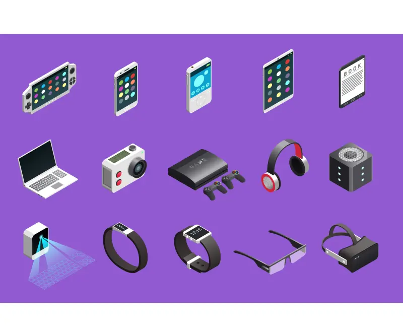
Table of Content
- I. Wearable Devices: Miniaturization Meets Ergonomics
- II. Internet of Things (IoT): The Network Behind the Node
- III. Smart Home Devices: Seamless Automation and Intelligence
- IV. Advanced PCB Technologies: The Blueprint for Tomorrow's Electronics
- V. Conclusion: Charting the Course Forward
- PCB Terminology Glossary
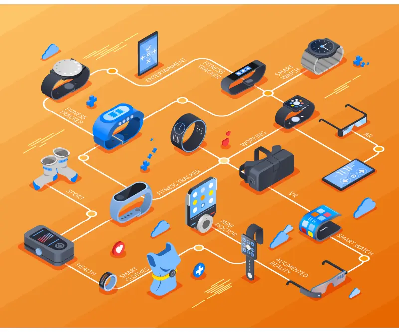
I. Wearable Devices: Miniaturization Meets Ergonomics
The wearable electronics market is driven by a relentless push for devices that are smaller, lighter, and more powerful than their predecessors. Devices like smartwatches, medical patches, and augmented reality glasses demand an unprecedented level of functionality packed into compact, ergonomic form factors that conform to the human body.
A. The Relentless Push for Miniaturization
The primary solution to the miniaturization challenge is the adoption of High-Density Interconnect PCBs (HDI) . Unlike traditional rigid boards, HDI PCBs use advanced manufacturing techniques to create finer traces and smaller vias—tiny holes that connect layers—allowing for higher component density within a smaller footprint. Features such as microvias and every-layer interconnection (ELIC) are essential for cramming more circuits into less space, making them the standard for modern smartphones and tablets as well as wearables. In HDI boards, the miniaturization extends to component selection, with designers opting for compact, surface-mount components like Chip-Scale Packages (CSPs) and Ball Grid Arrays (BGAs) to reduce the overall footprint of critical components.
B. Flexible PCBs: Design Freedom and Physical Adaptability
Beyond mere miniaturization, wearable devices require physical adaptability. This is where flexible PCBs (FPCBs) and rigid-flex PCBs become indispensable. Made from pliable materials like polyimide (PI), these circuit boards can bend, twist, and fold without compromising their electrical integrity, making them ideal for devices that conform to curved surfaces, such as a wristband or smart clothing. The engineering behind these boards is a balancing act of flexibility and reliability. A crucial design rule is the concept of "bending radius," which defines the tightest curve a board can make without damaging the traces or materials. For applications with repeated movement, industry standards recommend a minimum bending radius of at least 10 times the board's thickness. Additionally, designers must use curved or teardrop-shaped traces and avoid placing vias in bend zones to distribute stress evenly and prevent signal loss.
Flexible PCBs offer significant advantages, including space efficiency, weight reduction, and durability against constant mechanical stress and vibrations. They can reduce the need for bulky connectors and cables, leading to lighter, more comfortable devices. However, the use of advanced flexible technologies comes with a critical trade-off. While rigid-flex PCBs are often considered the technically ideal solution for devices that require both rigid circuitry and flexible connections, community discussions among engineers reveal a practical reality: their high cost can make them commercially unviable for mass-market consumer products. This is why many designs compromise by using a small, rigid PCB with all the primary components, enclosed within a flexible casing. This dichotomy highlights the ongoing tension between achieving engineering perfection and meeting market viability.
Looking to design flexible or rigid-flex PCBs? NextPCB offers advanced manufacturing services to help you overcome challenges and turn your innovative wearable designs into reality.
C. Thermal and Environmental Management in Compact Designs
The compact, tightly packed nature of wearable PCBs creates a significant challenge in thermal management. Excessive heat in a small, enclosed space can degrade component performance, shorten battery life, and even cause user discomfort. To combat this, designers employ specific PCB strategies, such as using thermal vias—small holes filled with a conductive material like copper—to transfer heat away from high-power components to internal layers or external heat sinks. Strategic component placement is also paramount; by distributing heat-generating parts across the board, engineers can prevent the formation of localized "hotspots".
Additionally, the PCB design must account for the physical stresses and environmental exposure of being worn on the body. A device for an active lifestyle needs to be durable against constant motion and moisture. Solutions include applying a conformal coating to protect the board from dust and environmental contaminants. From an ergonomic standpoint, the physical properties of the PCB directly impact the user experience. A board that is too heavy or generates too much heat can make a device bulky and uncomfortable, leading to product failure. This reality means that a successful PCB design is no longer judged solely on its electrical performance, but also on its contribution to the overall comfort and feel of the product.
To help visualize these complex relationships, the following table summarizes the key challenges and the expert-level solutions discussed.
|
Challenge |
Impact on Device |
Key Design Solutions |
|
Miniaturization |
Limits functionality; increases heat. |
HDI PCBs, smaller components (CSPs, BGAs), multi-layer boards. |
|
Low-Power Consumption |
Short battery life; frequent charging. |
Low-power components, PMICs, power-gating, efficient layout. |
|
Data loss, poor performance, interference. |
Proper stack-up, impedance matching, short traces, differential signaling. |
|
|
Thermal Management |
Overheating, degraded performance, user discomfort. |
Thermal vias, heat spreaders, strategic component placement, thermally conductive materials. |
|
Durability/Reliability |
Susceptibility to environmental stresses, mechanical failure. |
Flexible PCBs, conformal coating, robust materials (polyimide). |
|
Interference with other devices, regulatory failure. |
Solid ground planes, shielding, proper grounding, EMI filters. |
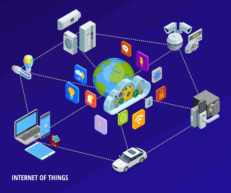
II. Internet of Things (IoT): The Network Behind the Node
IoT devices form a vast network of connected sensors and actuators, from industrial monitors to smart agriculture systems. The design philosophy for these devices diverges from wearables by prioritizing connectivity, longevity, and low-power operation, especially when devices are deployed in remote or inaccessible locations.
A. The Quest for Low-Power Longevity
For many IoT applications, the most critical design priority is low power consumption, allowing a device to operate for months or even years on a single battery. The PCB is central to this objective. Efficient PCB design for low power involves selecting components that consume minimal energy, such as microcontrollers (MCUs) with deep sleep modes that draw less than 1 μA in standby. A well-designed PCB layout complements this by incorporating Power Management ICs (PMICs) and implementing power-gating techniques, which selectively turn off power to parts of the circuit that are not in use. In single-layer PCB designs, designers must use wider traces for power lines to handle higher currents with minimal resistance and keep signal traces as short as possible to reduce power loss and signal delay.
This emphasis on longevity also highlights the crucial collaboration between hardware and software. While an efficient PCB layout is essential, it is a foundation, not the complete solution. A device's long-term power efficiency is ultimately determined by its firmware. By using dynamic voltage scaling, strategically keeping wireless modules off when not in use, and implementing deep sleep modes, software can dramatically reduce the average current draw and extend battery life from days to months or years. The hardware enables, but the software optimizes.
B. Connectivity and Signal Integrity
The promise of IoT lies in its ubiquitous connectivity. Devices must seamlessly communicate using a variety of protocols like Wi-Fi, Bluetooth, Zigbee, and cellular networks. However, with multiple communication modules and high-speed data transfer, the physical reality of the PCB becomes a major factor. The integrity of the electrical signals is paramount, as a single design flaw can compromise the entire value proposition of the device.
Common signal integrity issues include crosstalk, where signals on one trace interfere with signals on an adjacent trace; reflections, caused by impedance mismatches; and ground bounce, which can degrade signal quality. These problems can lead to data loss or device malfunction. To mitigate these risks, designers must implement expert-level strategies. This includes using a proper layer stack-up with an uninterrupted reference plane to provide a clear re
Additionally, careful routing, such as shortening parallel trace segments and spacing signal groups appropriately, is essential for minimizing crosstalk. On-board antennas, which save space and cost, also require meticulous layout to ensure optimal signal performance and a 50-ohm impedance match.
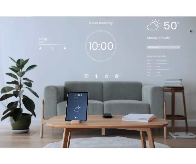
III. Smart Home Devices: Seamless Automation and Intelligence
The smart home ecosystem relies on a complex interplay of voice-controlled assistants, automated appliances, and interconnected sensors. For these devices, the PCB must provide not only seamless connectivity but also unyielding safety, long-term reliability, and compliance with strict standards.
> Recommend reading: Develop your Matter Smart Home Device with Beetle ESP32-C6 for Free - NextPCB Accelerator #3

A. Ensuring Safety and Performance Through EMC
In a densely packed electromagnetic environment with Wi-Fi routers, smart speakers, and other appliances, Electromagnetic Compatibility (EMC) is not an option; it is a critical safety and reliability requirement. EMC is a device's ability to operate in its electromagnetic environment without causing or being susceptible to interference (EMI).
PCB designers must account for both emitted and absorbed interference. This includes limiting noise from internal components like clock signals and power supplies, as well as ensuring the device can function without error when exposed to external interference from other devices or natural sources. To achieve compliance, designers use specific strategies, such as creating a solid ground plane for shielding, carefully placing components to avoid signal coupling, and managing trace lengths and impedance. Compliance with international regulations, such as the FCC in the U.S. and CE marking in Europe, is mandatory for commercial sale and avoids costly legal issues, product recalls, and reputational damage. This is a key distinction between a hobbyist project and a consumer-grade product. While a DIY smart thermostat may function perfectly on a bench, a professional product must be designed with the rigor to pass commercial EMC and safety tests.
B. Integrating Sensors and Actuators
Smart home devices operate by taking input from sensors and translating it into action through actuators. A PCB must be able to manage this delicate flow. For instance, a PCB for a smart blind motor needs to handle high-current motor circuits while simultaneously maintaining clean analog signals from a position sensor.
This dual requirement poses a complex design challenge. The board must be constructed to provide dedicated power planes for high-current components and separate them from sensitive analog sections to prevent electromagnetic interference. Thermal management is also critical, as actuators often involve high-power components that generate significant heat. Robust strategies, including the use of thermal vias and strategic component placement, are essential to ensure long-term reliability and prevent overheating. The PCB for a smart home device is a physical manifestation of a system that senses, processes, and acts, and its design must meticulously accommodate all three functions to deliver on the promise of seamless automation.
Worried about signal integrity issues? Choose NextPCB's professional design and manufacturing services to ensure your IoT devices perform flawlessly.
Fast PCB Assembly Services from China
IV. Advanced PCB Technologies: The Blueprint for Tomorrow's Electronics
The core challenges in wearables, IoT, and smart homes—from miniaturization and power management to thermal dissipation and EMC—are not unique to each domain. The solutions are converging on a set of advanced PCB technologies that are the blueprint for tomorrow's electronics.
- High-Density Interconnect (HDI) Boards: As a fundamental enabler of miniaturization, HDI boards are central to a future of smaller, more functional devices. They allow for more components to be packed into a smaller space using microvias and finer traces, which also enhances signal integrity by shortening signal paths. For high-complexity designs, HDI can even reduce the number of board layers required, making it more cost-effective than an equivalent standard board.
- Rigid-Flex PCBs: This technology is driving a paradigm shift in design, moving from a two-dimensional layout to a three-dimensional one. By combining rigid and flexible sections, a single circuit can be designed to bend and fold around a device's enclosure, eliminating the need for bulky connectors and cables. This not only increases durability and reliability but also enables innovative, non-traditional device shapes. The design process for rigid-flex boards requires close collaboration between electrical and mechanical engineers and the use of advanced 3D simulation tools.
- Embedded Passive Technology: This technique involves integrating passive components, such as resistors and capacitors, directly into the inner layers of the PCB substrate. This frees up valuable surface area for active components and more complex routing, which is critical for miniaturization. Furthermore, by placing components closer to the circuits, embedded passives reduce parasitic capacitance and inductance, leading to improved electrical performance and reduced signal noise, particularly at high frequencies. The resulting board is also more durable and resistant to shock and vibration as it has fewer solder joints.
These converging technologies point to a future where the PCB designer must be a versatile generalist, mastering these core enabling technologies to remain competitive in any of these markets.
The following table provides a comprehensive overview of how these advanced PCB technologies address the needs of each domain.
|
Technology |
Primary Benefit |
Common Applications |
Core Design Challenges Addressed |
Key Drawbacks |
|
High-Density Interconnect (HDI) |
Miniaturization, enhanced signal integrity. |
Smartphones, wearables (smartwatches), medical devices. |
High component density, signal integrity, heat dissipation. |
Requires advanced manufacturing, higher initial cost. |
|
Rigid-Flex |
3D design freedom, improved reliability. |
Medical implants, wearables (fitness trackers), aerospace. |
Durability, mechanical stress, elimination of connectors. |
High manufacturing cost, complex design rules. |
|
Flexible PCB (FPCB) |
Ergonomics, weight reduction, bending. |
Smart clothing, medical patches, fitness trackers. |
Conforming to a curved surface, reduced weight, durability. |
Fragility during assembly, component strain. |
|
Embedded Passives |
Space efficiency, improved electrical performance. |
Mobile devices, wearables, IoT sensors. |
Miniaturization, parasitic effects, signal integrity. |
Cannot be replaced if defective, higher design complexity. |
V. Conclusion: Charting the Course Forward
The analysis presented in this report confirms that PCBs are the silent, yet essential, foundation of modern electronics. Without the continuous innovation in PCB design and manufacturing, the seamless functionality of wearables, the long-term autonomy of IoT devices, and the reliable intelligence of smart homes would be impossible. The challenges inherent in each domain—from the thermal management of a compact wearable to the EMC compliance of a smart home hub—are not obstacles but rather fertile ground for engineering innovation.
The future of these industries will be defined by a convergence of advanced PCB technologies. High-Density Interconnect (HDI) boards, Rigid-Flex PCBs, and Embedded Passive Technology are becoming the universal solutions to the most pressing design problems. These technologies not only enable the next wave of smaller, more powerful devices but also fundamentally change the design process itself, demanding a shift from two-dimensional to three-dimensional thinking and a greater collaboration between electrical and mechanical engineering disciplines. The road ahead for engineers and designers involves embracing these new technologies, staying informed about emerging trends like sustainable manufacturing and stretchable electronics, and participating in the collaborative, problem-solving spirit that defines these forward-looking industries.
Bring your electronic devices from concept to market with NextPCB. Whether you're validating a wearable, scaling an IoT node, or hardening a smart-home hub, our HDI, rigid-flex, and turnkey assembly services cover the full NPI cycle—prototype to production.
> Start your PCB prototype >> Learn Fast PCB Prototype Services
> Request turnkey PCB assembly >> Learn Turnkey PCB Assembly Service
> Get a free DFM review >> Try NextPCB Free Online Gerber Viewer or Download HQDFM Instantly
PCB Terminology Glossary
|
Term |
Definition |
|
HDI (High-Density Interconnect) |
A PCB technology that uses fine traces, smaller vias (microvias), and high component density to allow for more functionality in a smaller footprint. |
|
FPCB (Flexible Printed Circuit Board) |
A circuit board made from a flexible polymer film, such as polyimide, that can bend, twist, and fold. |
|
Microvia |
A very small drilled hole, typically less than 150 micrometers in diameter, that connects layers in an HDI PCB. |
|
EMI/EMC (Electromagnetic Interference/Electromagnetic Compatibility) |
The ability of a device to operate without causing or being susceptible to electromagnetic disturbances. EMI is the disturbance itself, while EMC is the state of a device's ability to handle it. |
|
Via-in-Pad |
A microvia that is placed directly within the copper pad of a component, reducing signal path length. |
|
BGA (Ball Grid Array) |
A type of surface-mount component package that uses a grid of solder balls on the underside of the package for electrical connection. |
|
Power-Gating |
A technique used in low-power PCB design where power to parts of the circuit is selectively turned off when not in use to conserve energy. |
|
Thermal Via |
A small hole in a PCB, typically plated or filled with copper, used to transfer heat away from a component to other layers or a heat sink. |
|
Substrate |
The base material of a PCB, such as FR-4 or polyimide, that provides mechanical support and electrical insulation. |