
 NextPCB Capabilities
Printed Circuit Boards
NextPCB Capabilities
Printed Circuit Boards
 PCB Assembly
 Layer Buildup
 SMD-Stencils
 PCB Design-Aid & Layout
 Mechanics
 Quality
 Drills & Throughplating
 Factory & Certificate
 PCB Assembly Factory Show
Certificate
PCB Assembly Factory Show
Certificate
Support Team
Feedback:
support@nextpcb.com


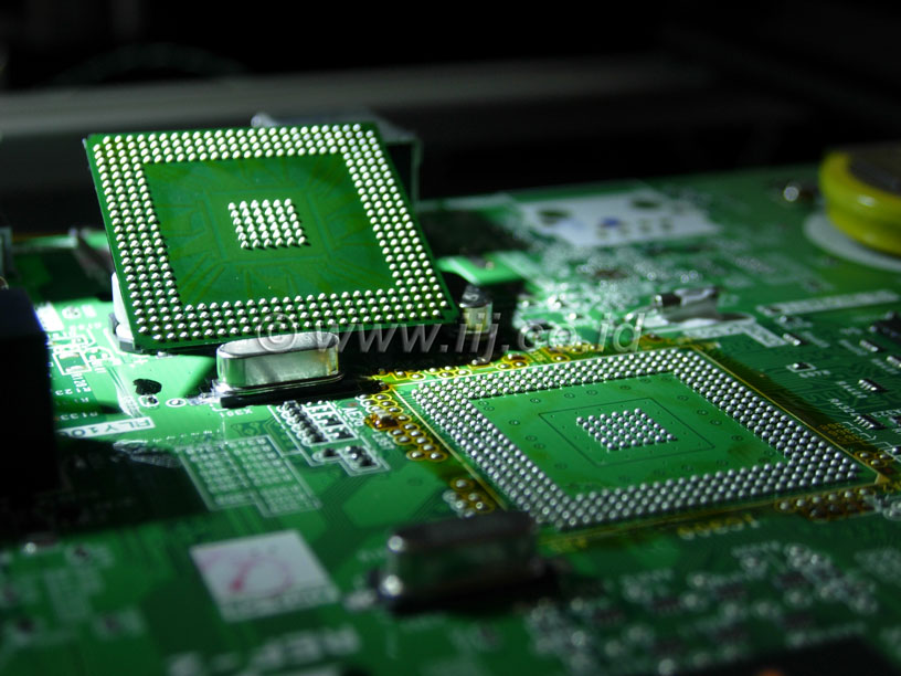
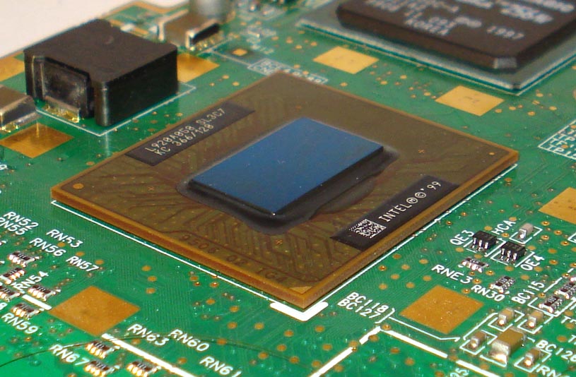
When it comes to extremely sensitive computer parts. It is identifiable that connecting the integrated circuits through the wires is hard when it comes to the surface-mounted components. The ball grid array is the best solution for this. These BGA can be easily identified at the bottom of the microprocessors. Since this directly connects the terminals, the BGA is highly considered in the development of computer parts and other high-performance computational machines. The BGA uses the total component's full area, giving more space for connections and good communication.
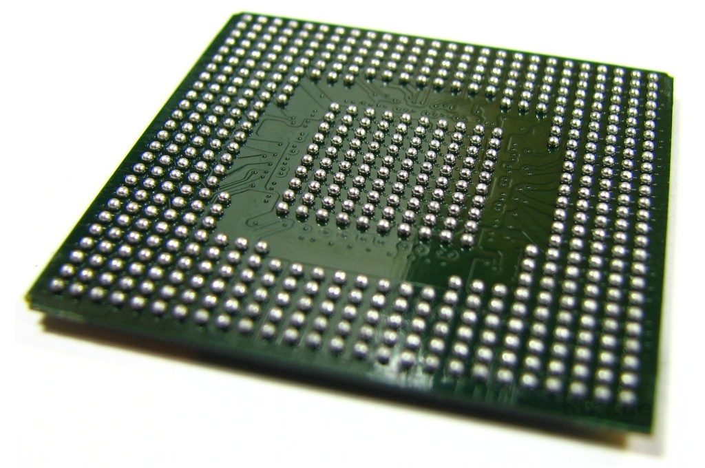
BGA is an acronym for Ball Grid Array. This is, in general, a collection of little, tiny metallic conductor balls that are put harmoniously on the board as we move toward creating a printed circuit board (PCB).
The Ball Grid Array, or BGA, has a different connecting strategy than typical surface mount connectors. Another packaging, such as the quad flat pack (QFP), included connectors on the sides of the package. This meant that there was little space for the pins, which had to be closely spaced and significantly shrunk to offer the necessary amount of communication. The BGA employs the package's underside, where there is ample space for connections.
The ball grid array is gaining popularity among SMD ICs that require dense connections. Using the underside of the IC package instead of connections around the edge makes it possible to reduce connection density, hence facilitating PCB layout.
Using the underside of the chip prevents direct access to the connections, which makes soldering, desoldering, and inspection more challenging. In such high-density packages, correct solder mask design rules in the Gerber file become especially critical to avoid bridging and poor joint formation.
The superior thermal dissipation performance of BGA keeps the core cool during operation, hence extending the product's lifespan. Heat is the most crucial factor to consider, and BGA is the reason why technology goods operate so efficiently while maintaining a normal temperature even when operating at full capacity.
The second most essential factor is the electrical characteristics. The shortest distance connections with the lowest feasible resistive paths increase the value and importance of BGAs.
The third most essential factor is compatibility. Being able to utilize the shortest space while dealing with a bigger number of balls enables the producer to include an increasing number of workable choices. Hence increasing the product's value and desirability.
BGAs are the heart of the things you wish to manufacture. This relies not only on the sort of products you wish to manufacture. But also on the entire production cost, the weight of the final product, the quality of the product, the amount of heat generated, and a host of other factors.
This is ceramic BGA type. In this type, the ratio between tin and lead is 10:90. This type of BGA requires C4 Approach (Controlled Collapse Chip Connection) for constructing the bridge between BGAs and PCBs. It is due to its extremely high melting point. This type of BGA is more expensive than PBGAs, but it is incredibly dependable for improved electrical performance and thermal conductivity.
The abbreviation for Plastic Ball Grid Array is PBGA. This is the most prevalent type of double-sided PCB now in use. MOTOROLA becomes credited with pioneering it, although currently, virtually all producers make use of it. As the substrate material, bismaleimide triazine (BT) resin forms the core. This, together with the application of over-molded pad array carrier (OMPAC) sealant technology or glob-to-pad array carrier (GTPAC), and proven by JEDEC as being highly dependable (Level 3). These BGAs contain between 200 and 500 ball arrays.
The only disadvantage of TBGA is that it is always more expensive than PBGA. However, TBGA is the best choice for thin goods. That requires robust core materials, superior heat dissipation, and superior electrical connectivity. Whether the ICs / Chips must be facing up or down, this is the strategy for maximizing product value while minimizing costs. In this form of BGA, wire bonding is usually preferred if the chips are facing up, but the flip-chip technique seems suited if the chips are facing down.
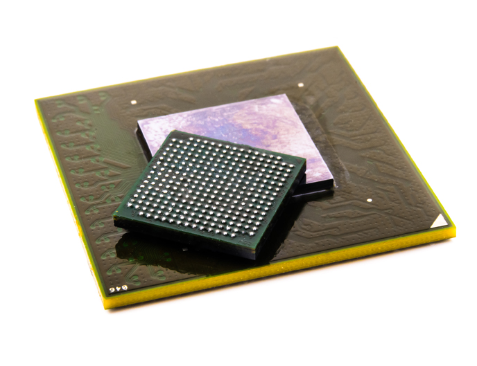
The package on package (PoP) is a packaging approach for integrated circuits that combines vertically discrete logic and memory BGA units. Stacking refers to the installation of two or more packages atop one another with a standard interface to transport signals between them.
PoP technology exists to meet the electronics industry's continual demands for fine pitch, smaller size, high signal processing speed, and lower mounting space in electronic products such as smartphones and digital cameras. Using this technique in the PCB assembly process, memory devices in the top package and logic devices in the bottom package are electrically connected and are tested and replaced individually. All of these qualities lower the cost and complexity of PCB construction.
The Land Grid Array, or LGA, is a package that uses metal pads instead of leads (as in the pin grid array) or solder balls for external electrical connection (as in the ball grid array). These metal pads, known as "lands," are typically organized in a grid or array at the package's base, hence the name "land grid array." The grid-like design of the LGA package's lands enables it to have a large land count, making it a common packaging option for devices with extensive I/O needs.
Land counts for typical LGAs range from 8 to 1681. LGAs with the lowest land counts are essentially QFNs, as the lands of these packages are confined to the body's periphery. Typical LGA land pitch (distance between lands) values range from 1.0 mm to 1.27 mm.
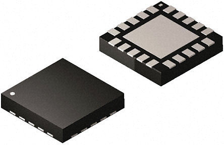
Connecting the ASCIC to the PCB is the QFN semiconductor package. Moreover, it accomplishes this via surface-mount technology. In addition, the QFN is a lead-framed packaging known as a Chip Scale Package (CSP). And this is due to the fact that it enables you to observe and contact leads after assembly. Typically, the PCB connectivity and die assembly of QFN packages typically comprised of a copper lead frame. In addition, this package may feature a single or numerous row of pins.
The QFN packaging has a die wrapped by a lead frame. The lead frame consists of a copper alloy with a tin covering that is matte.
Wire bonding is typically utilized to connect the die and the frame. Copper/gold is typically preferred for bonding wires. Some manufacturers implement this interface using flip-chip technology. The flip-chip method provides superior electrical performance in comparison to the conventional method.
On the underside of the device are the metalized terminal pads. Along the four borders of the bottom surface, these terminal pads offer electrical connectivity to the PCB.
On the bottom of the packaging is a pad that is exposed. This pad provides a heat-conductive channel to the PCB. The exposed pad also allows for ground connection. At the exposed pad, the QFN package becomes soldered to the circuit board. Die to attach refers to the epoxy used to secure the die to the exposed pad.
Comparable to CBGA, except for the ceramic substrate. This FC-BGA instead utilizes BT resin. In this manner, the additional expense becomes minimized for this type. The primary benefit derives from the shorter electrical pathways compared to other BGA varieties, resulting in superior electrical conductivity and increased performance speed. The ratio of tin to lead in this BGA type is 63:37. The chips utilized on the substrate can easily realign to the correct place without the usage of a flip-chip alignment machine, which is another advantage of this BGA kind.
The Ball Grid Array originally created to provide a number of advantages to IC and equipment producers, as well as to equipment users. Among the advantages of BGA over other technologies are the following:
There are numerous reasons why current technology relies heavily on BGA. The most crucial is that BGA offers superior thermal dissipation. It allows the core to remain cool during operation and so extending the product's lifespan. Heat is the most crucial factor to consider, and BGA is the reason why technology goods operate so efficiently while maintaining a normal temperature even when operating at full capacity.
The second most essential factor is the electrical characteristics. The shortest distance connections with the lowest feasible resistive paths increase the value and importance of BGAs.
The third most essential factor is Compatibility. Being able to utilize the shortest space while dealing with a bigger number of balls enables the producer to include an increasing number of workable choices, hence increasing the product's value and desirability. This indirectly contributes to reducing production costs while producing more valuable and affordably priced goods for production and market clients.
Still, need help? Contact Us: support@nextpcb.com
Need a PCB or PCBA quote? Quote now


 Surface

