
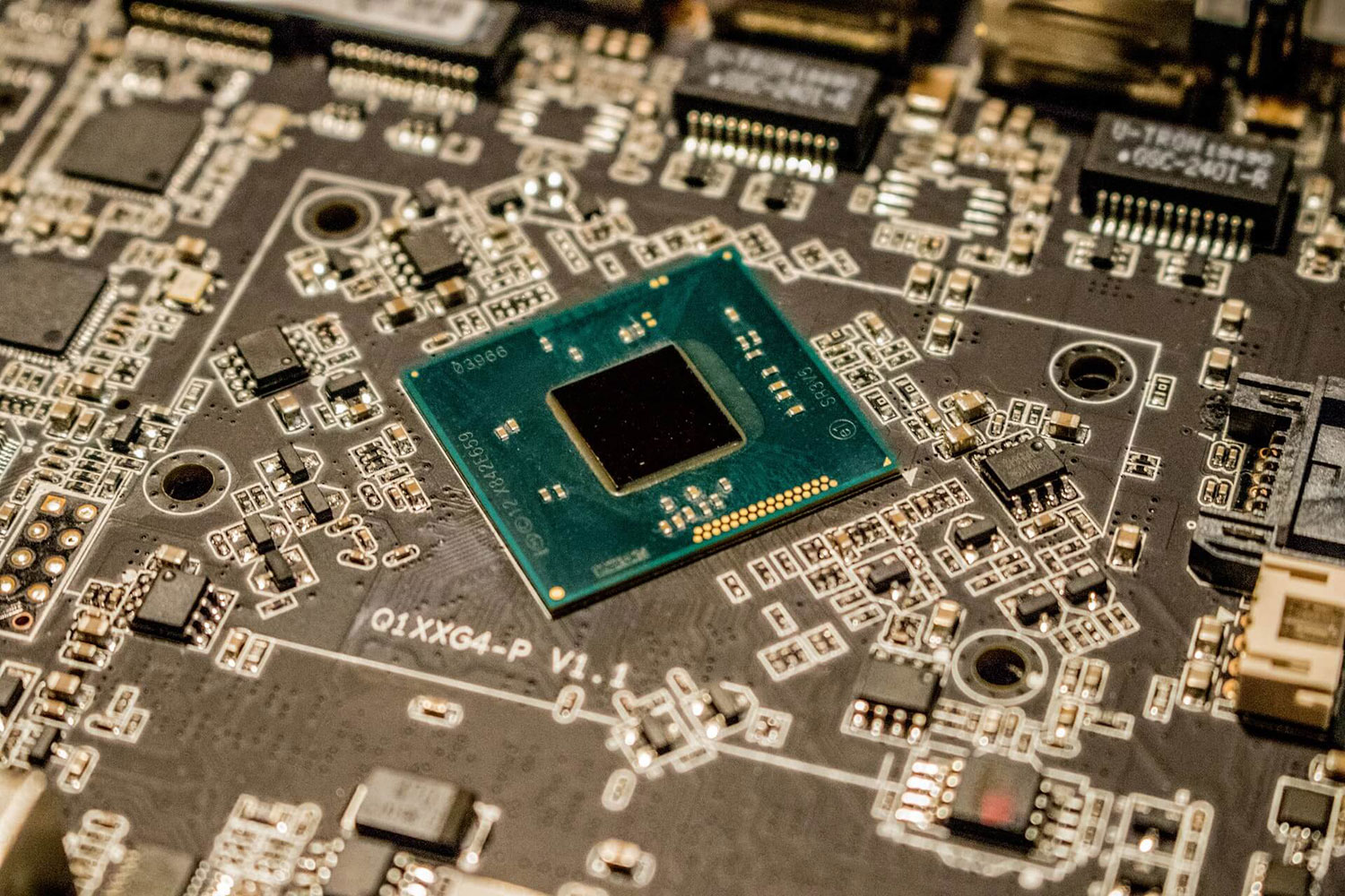
 NextPCB Capabilities
Printed Circuit Boards
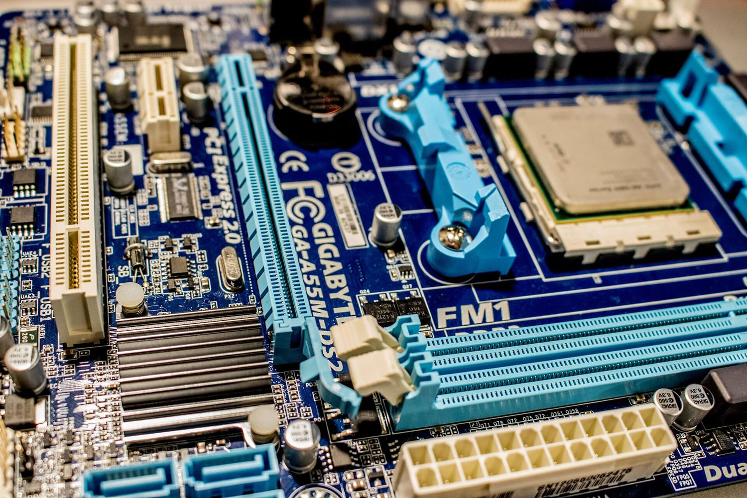
NextPCB Capabilities
Printed Circuit Boards
 PCB Assembly
 Layer Buildup
 SMD-Stencils
 PCB Design-Aid & Layout
 Mechanics
 Quality
 Drills & Throughplating
 Factory & Certificate
 PCB Assembly Factory Show
Certificate
PCB Assembly Factory Show
Certificate
Support Team
Feedback:
support@nextpcb.com


Engineers use blind and buried vias from a number of techniques to increase the high-density interconnect in printed wiring boards (PWB). Blind and buried vias will work if you don't want to go all the way through the printed board. They also go only partially through the multilayer circuits, connecting only the internal layers that need to be connected.
NextPCB now offers HDI boards, one of the PCB technologies with the quickest rate of growth. HDI Boards frequently have microvias with a diameter of 0.006 or less and may also have blind or buried vias. Compared to conventional circuit boards, they have more circuitry density. In this article, we will briefly explain everything related to high-density interconnect in PWBs and PCBs.
High-Density Interconnect (HDI) is a printed circuit board (PCB) technology that allows for a higher density of components to be placed on a smaller area of the board. HDI technology enables designers to fit more functionality and features onto a single board while reducing the overall size of the PCB.

The development of printed circuit boards has kept pace with the need for smaller and faster products as technology has changed. The vias, pads, copper traces, and gaps on HDI boards are all smaller. Due to their denser wiring, HDI PCBs are smaller and lighter than traditional PCBs and require fewer layers. As a result, a single HDI board can often replace multiple PCBs in a device, streamlining its design and reducing its weight and size.
Manufacturers divide the HDI boards into six different categories:
Technology must adapt to changing consumer needs. Designers now have the ability to add extra components to both sides of the raw PCB by utilizing HDI technology. Multiple via techniques, such as blind via and via in pad, provide designers extra PCB space to cram tiny components even closer together. Engineers accommodate more I/O in smaller geometries due to small component size and pitch. As a result, signal transmission times will be shorter and signal loss and crossing delays will both be significantly reduced.
Although certain consumer goods have shrunk in size, quality continues to be the consumer's top concern, followed by price. Engineers can condense an 8-layer through-hole PCB into a 4-layer HDI microvia technology packed PCB by using HDI technology during design. A well-designed HDI 4-layer PCB's wiring capabilities can perform comparable or superior tasks to those of a conventional 8-layer PCB.
Even if the PCBs cost is increased by the microvia process, the cost of material square inches and layer count is greatly decreased with good design and layer count reduction.
It is cost-effective as when engineers properly plan, overall costs decrease. It is because normal PCBs have fewer layers due to perfect design efficiency in HDI PCB manufacturing. The design and testing processes for HDI PCBs are quicker due to the simple placement of components and vias as well as electrical performance. Further better reliability in microvias, which have a smaller aspect ratio than conventional through holes, are more trustworthy than through holes and give HDIs superior performance with better materials and parts.
There are a few small but significant ways in which the HDI manufacturing process differs from the conventional PCB manufacturing process. It's crucial to note that fabricator constraints will restrict design freedom and place restrictions on the board's routing. Although your design software can still support the use of thinner traces, smaller vias, more layers, and smaller components.
But doing so means you're applying design for manufacturing (DFM) requirements by automotive techniques. The manufacturing procedure and materials utilized to construct the board will determine the precise DFM requirements. When engineers consider reliability, then DFM requirements also become significant.
Due to advanced technology, now designers can create multilayer PCB by sequentially adding more pairs of layers. Now with the help of a laser drill engineers can create holes in the internal layers that allow plating, imaging, and etching prior to pressing. And sequential build-up is the name engineers assign to this additional phase. Engineers use solid-filled vias during SBU fabrication, which improves heat control, creates a stronger interconnect, and increases board reliability.
The material's performance in terms of temperature resistance, adhesion, tensile strength, flexibility, dielectric strength, dielectric constant, and several other physical, electrical, and thermal characteristics must be taken into account. The material used to construct the PCB has a direct impact on the PCB's performance and degree of integration. That's why engineers use materials from two categories to design PCBs.
Thermoset materials have high melting points, but when they are exposed to a specific temperature and solidified, their parts and physical characteristics are fixed. They cannot transform back into their original forms or meltdown. Thermosets are composed of resins like aramid, epoxy, and polyimide.
Thermoplastic materials have low melting temperatures and when you heat them, they will either soften to a flexible condition or melt into a liquid form. They can mold into almost any form or pattern. Even very high temperatures cannot alter the composition of the substance. Thermoplastics are typically based on PTFE and filled with organic or inorganic materials.
Further, engineers employ nine different types of general dielectric materials in HDI substrates. Many of them are covered by IPC slash sheets like IPC-4101B and IPC-4104A, while many are not yet described by IPC standards. The materials list is:
Engineers created resin coated copper in order to help with poor hole quality, prolonged drill times, and to enable thinner PCBs. And engineers use RCC which has a very low profile along with copper foil that is very thin and is attached to the surface with tiny nodules. The material has undergone chemical processing to prepare it for the thinnest and most precise line and spacing technology.
Manufacturers still use heated roll technology to apply the dry resist to the laminate's core material. Now, engineers advise preheating the material to the desired temperature before the lamination procedure for HDI PCBs. Preheating the material makes it easier to apply dry resistance evenly to the laminate's surface, which transfers less heat away from the hot rollers and maintains stable exit temperatures for the laminated product. And engineers trap less air beneath the film due to consistent entrance and exit temperatures, which is essential for the reproduction of fine lines and spacing.
Assembly, PWB, and component are the three key components that makeup interconnection density. While their full extent is not always evident, we shall utilize additional charts and graphics to describe and comprehend interconnect density.
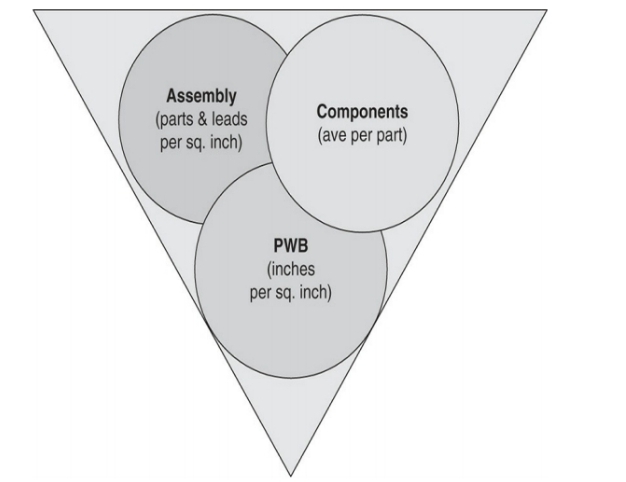
In the diagram, designers illustrate the connection between PWB density, surface mount technology (SMT) assembly, and component packing. The connections between these three things are apparent and unmistakable. Any adjustments to any one of them have a major impact on the connection density overall.
Engineers can determine how challenging it is to assemble surface-mounted components by measuring assembly complexity in terms of leads and parts per square inch.
Manufacturers use component packaging complexity to gauge the average leads (I/Os) per portion of a component's sophistication.
PWB's total area, including all signal layers, or the average length of traces per square inch, is divided by the number of wires on that board.
The picture depicts the effect of PWB, assembly, and component technologies on overall package technology and density.
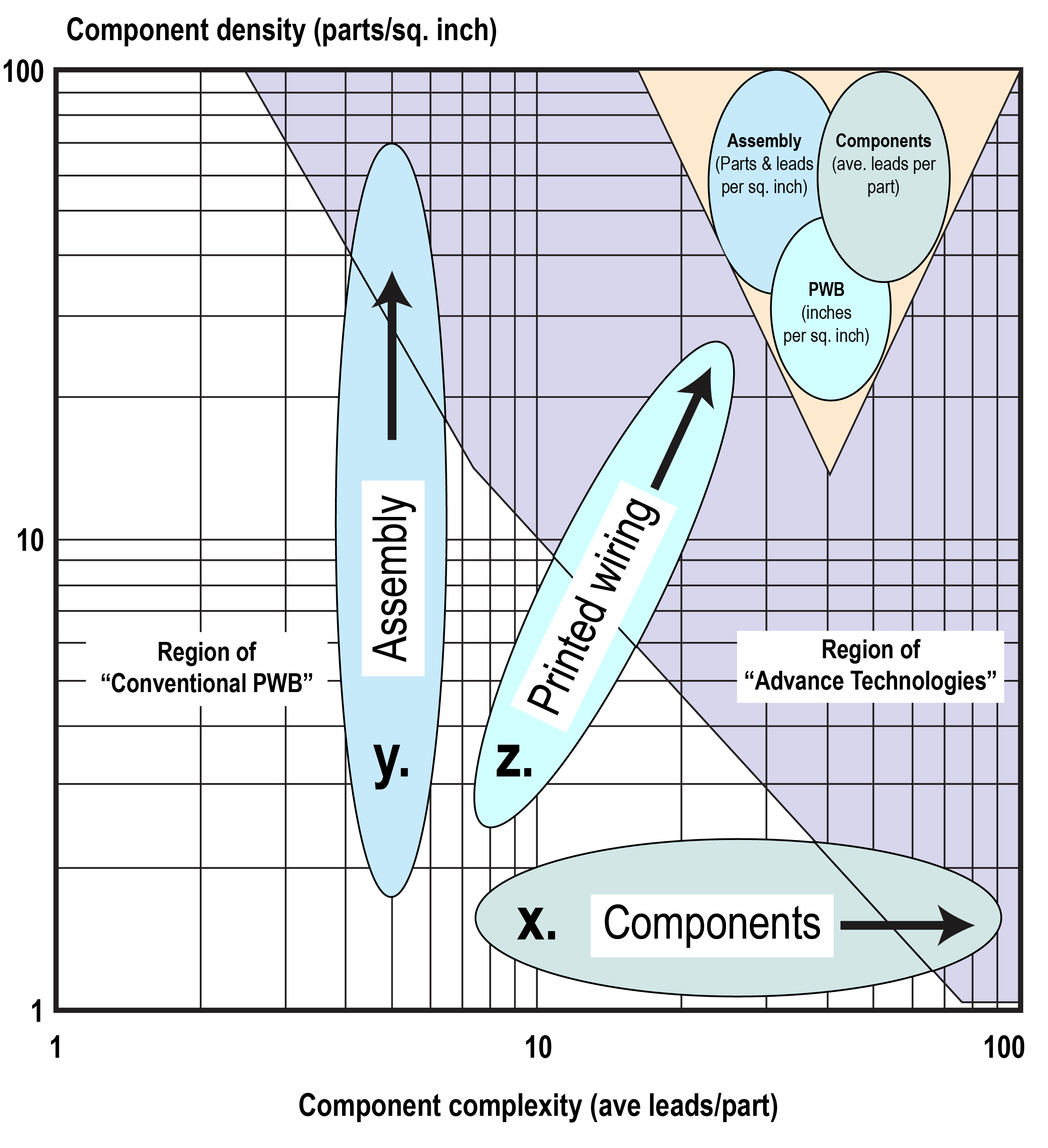
The interconnection density is the barrier that divides PWB technologies from HDI technologies, as further explained by the above graphic. On the one hand, using traditional PWB technology in this way maximizes cost-effectiveness. On the other side of the HDI wall, HDI technologies eventually become more affordable.
A little discussion of the electronic systems' packaging hierarchy will be helpful. It is essential to know how PWBs will adjust within them with the proper perspective.
In electronic Circuits (IPC), engineers introduced eight different types of system components in descending order of size and complexity. For better comprehension, let's define categorical decisions, but before we do, let's attempt to grasp the concept of hierarchy.
Generally speaking, the term "hierarchy" refers to an organizational structure in which items are ranked according to some standard, usually based on levels of importance. Hierarchical systems come in a variety of forms in computers, and electronic packaging, etc. For instance, most file systems use a hierarchical structure to assign files to specific locations. Below is the categorical packaging division of interconnections in Printed Wiring Boards.
Category A includes thoroughly processed active and passive devices. Uncased or naked chips, discrete capacitors, resistors, or their networks, etc. are typical instances of this category.
Category B includes all packaged devices (both active and passive), both active and passive, with plastic packaging, such as DIPs, TSOPs, QFPs, and BGAs, as well as those with ceramic packaging, such as PGAs, connectors, sockets, and switches.
Category C substrates combine uncased or bare chips (i.e., category A components) into a package that is detachable. Additionally, this section covers all variations of multichip modules (MCMs), chip-on-boards (COBs), and hybrids.
It consists of substrates from categories B and C that join to form assemblies of already packed category D components. This category includes all rigid PWB types, discrete wiring boards, and flexible plus rigid-flexible boards.
Category E of the hierarchy system includes all printed wire, discrete wiring, flexible circuits, and other backplane fabrication methods that connect PWBs but do not include the parts from the aforementioned categories.
This includes RF plumbing, ground, and power distribution buses, coax or fiber optic line, harnesses, etc.
Card racks, electronic auto parts, thermal control parts, and hardware for system assembly are all packed in section G.
Category H applies to the entire system, which includes all of its bays, racks, boxes, and support subsystems.
Among the many above issues, the function and system of PWB design, as well as the parts types and the attributes to carry the system, all influence the packaging aspect of PWB design.
For example, the working conditions of the system, clock speeds, power use, and heat control techniques. This section contains a list of essential constraints that manufacturers should take into account while designing an electrical system's base PWBs.
The speed at which the electronic system operates is a critical scientific factor in the design of interconnections. Numerous digital systems already run at speeds higher than 100 MHz.
The quality of the materials used in PWB are under extreme demand from engineers. And intense pressure brought on by speeding up the system.
The attributes of the materials that designers intend to use must be understood by them. Because the square root of the dielectric constant of the materials has an inverse relationship with the speed of signal traveling.
If engineers want to make an operating system electronic friendly. Then the device director length should be cut down. Due to the fact that engineers use these device managers for signal transmission on the substrate between chips at fast speed.
Further, if the engineer wants to lessen warp and signal losses in systems operating at rates greater than 25 MHz. The interconnections must then have attributes of a transmission line, they should be aware of this. If the manufacturers want to deliver the high performance, precision, and optimal design then they should aware that transmission lines emphasize precise manufacture, conductor and dielectric separation parameters which they calculate with great care.
As clock rates and the number of gates on a chip increase, so does the power usage of the semiconductors. Engineers should be aware that chips require up to 30 W of electricity in order to operate. Because each chip has different power needs.
Therefore, if engineers want to provide energy and manage the return flow on the ground planes then they should need more terminals. Manufacturers take between 20 and 30 percent of chip terminals by power and ground connections. And if electronic signal detachment is necessary to boost system performance, the overall % could rise to 50%.
Therefore, engineers should include enough ground distribution and power planes when designing multilayer boards (MLBs). And it applies to devices that use 5 V or less than 3.3 V and consume tens of watts. Additionally, engineers can reduce unnecessary heat collection and Di/dt switching interference to boost up the systems. But how? Simply engineers can do this by dividing power ground throughout the system properly. Further, engineers randomly use separate bus-bar constructions to meet such high power needs.
If engineers want to ensure the system has a long life period and good performance. Then they must make sure that every bit of energy they send to power ICs to remove from the system. The process of eliminating heat from an electronic packaging system is one of the more difficult ones.
Huge heat-sink structures that can accommodate the individual integrated circuits needed to air-cool them are required for huge systems. Some computer firms have well-designed structures to use liquid cooling for their computer modules. In a number of computer architectures, engineers employ liquid immersion cooling. Large systems' cooling needs, however, put a strain on the performance of the available cooling methods.
Engineers working on packaging still need to reduce hot spots and ensure long-term performance. Despite the fact that smaller, movable, or tabletop electronic gadgets are less affected by the issue. The engineers should check the method of heat conduction through the board to avoid any errors. Because PWBs that employ techniques like thermal vias, placed metal slugs, and conductive planes have a bad reputation.
Engineers can use RF signal generators, ICs, modules, and a variety of assemblies. They also function as the frequency of operation of electronic devices increases.
Emissions of this kind that cause electromagnetic interference (EMI) offer a serious risk for mistakes, failures, and errors. Additionally, they are brought by neighboring electronics operating. Engineers must avoid them even with other parts of the same piece of equipment. The engineers outlined very low permissible amounts of this radiation in special EMI regulations.
Packaging engineers, and specifically PWB designers, need to be familiar with the methods for reducing or eliminating EMI radiation. And the purpose of this is to guarantee that their equipment won't create more power than is allowed.
The packaging strategy is controlled by two factors. The target market category and the application are both important for electrical products. The designers should understand the primary elements that affect the power of product usage. And designers are aware that it might be driven by prices, performance, or anything else. The gravity of each piece of equipment in Table 1 which contains a set of conditions is defined by the IPC.
TABLE 1. Realistic Representative-Use Environments, Service Lives, and Acceptable Cumulative Failure Probabilities for Surface-Mounted Electronics by Use Categories
| Worst-case use environment | |||||||
| Use category | Tmin, °C | Tmin, °C | ∆T*, °C | tD, h | Cycles/year | Years of service | Acceptable failure risk, % |
| 1-Consumer | 0 | 60 | 35 | 12 | 365 | 1-3 | ~1 |
| 2-Computers | +15 | +60 | 20 | 2 | 1460 | ~5 | ~0.1 |
| 3-Telecomm | -40 | +85 | 35 | 12 | 365 | 7-20 | ~0.01 |
| 4-Commercial aircraft | -55 | +95 | 20 | 12 | 365 | ~20 | ~0.001 |
| 5-Industrial & automotive | -55 | +95 | 20 | 12 | 185 | ||
| (passenger comparment) | &40 | 12 | 100 | ~10 | ~0.1 | ||
| &60 | 12 | 60 | |||||
| &80 | 12 | 20 | |||||
| 6-Military | -55 | +95 | 40 | 12 | 100 | ||
| ground & ship | &60 | 12 | 265 | ~5 | ~0.1 | ||
| 7-LEO | -40 | +85 | 35 | 1 | 8760 | 5-20 | ~0.001 |
| Space GEO | 12 | 365 | |||||
| 8-Military b | α | 40 | 2 | 365 | |||
| avionics c | -55 | +95 | 60 | 2 | 365 | ~10 | ~0.01 |
| 80 | 2 | 365 | |||||
| &20 | 1 | 365 | |||||
| 9-Automotive | 60 | 1 | 1000 | ||||
| (under hood) | -55 | +125 | &100 | 1 | 300 | ~5 | ~0.1 |
| &140 | 2 | 40 | |||||
Computers, consumer convergence, and communication technology have all advanced due to the universal digitization of electronic functions. This increased development allures the electronic industries. Additionally, there was plenty of guidance for the mass production of many electronic products. As a result, the cost of the final product is now the key factor in the design of every electronic system.
The design engineer must take into account all potential trade-offs in the context of the items' ideal performance solution. While following the above design and operation features. It is clear that the manufacturer decided to cover 60% of the early design costs. It emphasizes the importance of performance & trade-off analysis in electronic product design. Furthermore, everything is clear if the designer maintains 35% of the entire design.
Design for manufacturability and assembly (DFM/A), often known as paying attention to the needs and resources for manufacturing and assembly They can reduce PWB expenses by 25% and assembly costs by up to 35%.
The designers should follow the must most affordable electrical package designs:
The number of transistors per chip in digital integrated circuits is referred to as parts density (ICs). It keeps growing every year. Despite some engineers' claims that they will be able to have a single atom execute several functions, the physical volumes of individual atoms set a practical limit on component density.
Skilled engineers create a variety of measures to analyze and set relations between component density and PWB density. This is due to the fact that the parts and their terminations have a big influence on the PWB design. H. Holden, a famous writer, has completed a study of these connections.
Using this knowledge, you can assume PWB density and the location of the suggested product on the component density area.
In order to acquire the cheapest design, which is important for the right design of PWBs, we must first estimate the densities and then compare various board construction techniques. You should be aware that there are a number of basic words, expressions, and formulas to know and check the wire density of PWBs.
To determining the necessary wire density, till now, several engineers empirically develop different equations that allow calculating the demand for such wiring.
$$W_c=\frac{T*L}{G}\ in/in^2$$
Let's explain PWB equation formula in detail:
We will discuss each factor's effect on designing yields and on board costs, one at a time. If the methods for handling the first two conditions have failed to produce the appropriate board density, we resort to the final alternative, which is the easy but most expensive. Here is how you can increase interconnection density.
The main barrier to restrict an increase in the part channel size are wide pads around PTHs. Since PWBs still need pads that are broader than the parts at their location, technology is still not where it needs to be.
To analyze link density ID rightly, engineers must take into account the pads. Because the affinity that PCB boards can establish is prevented by these pads. For instance, in one design, lessening the pad widths from 55 to 25 mils (by 55%) can increase the connection density by 50%.
You can also reduce the device manager pitch Cp from 18 to 7 mils (a 61% decrease). Now, it should be clear to you that a more successful method to expand a pad's wire power is to completely reduce or remove it.
In order to account for any potential layer-to-layer or pattern-to-hole misregistrations, PWBs feature copper pads around the drilled holes. Additionally, it stops any holes from being left outside the pads' copper region. These are the two main reasons for the incorrect registration. These are the base laminate's instability and movement during PWB or multilayer board (MLB) production procedures.
Engineers should limit this movement to no more than 300 ppm, as per the basic features of the base material. However, in reality, base material decrease is closer to 500 ppm. Consequently, there was a layer shift of 10 mils over a 20-in span. There are too many applications for this temperature. In order to protect the area around drilled holes, a minimum 10-mil-wide annular ring should be present in the device manager.
It is easy to increase the number of wire channels on each signal plane by reducing the widths of devices and spaces. As engineers explain, it is a clear technique to increase PWB connectivity. Engineers using this strategy from a very long time in the IC and PWB industries.
But engineers also explain that you cannot lower the conductor widths and gaps. Especially when these conductors are lengthy, as they typically are on PWB density. Processing restrictions exist for this conductor reduction. Because production yields could suffer if the reduction pushes the process capabilities beyond their typical boundaries.
In addition, engineers know that the spaces between the conductors have limits to shrink. For instance, ensuring appropriate signal propagation conditions, small noise, limiting excessive crosstalk, and offering limits are some ways to adhere to limits.
Nevertheless, if carried out within the stated limits. Thus, increasing PWB density and reducing PCB manufacturing costs may be accomplished with such lessening conductors. By reducing widths from 6 to 3 mils, engineers can get the same connectivity for the number of signal layers.
Any actual increase in the conductor density Id in PWBs would only be accessible if production with yields was possible using the designing techniques. As seen in the image below, The yields of thin conductors reduce rapidly as PWB widths drop below 5 mils.
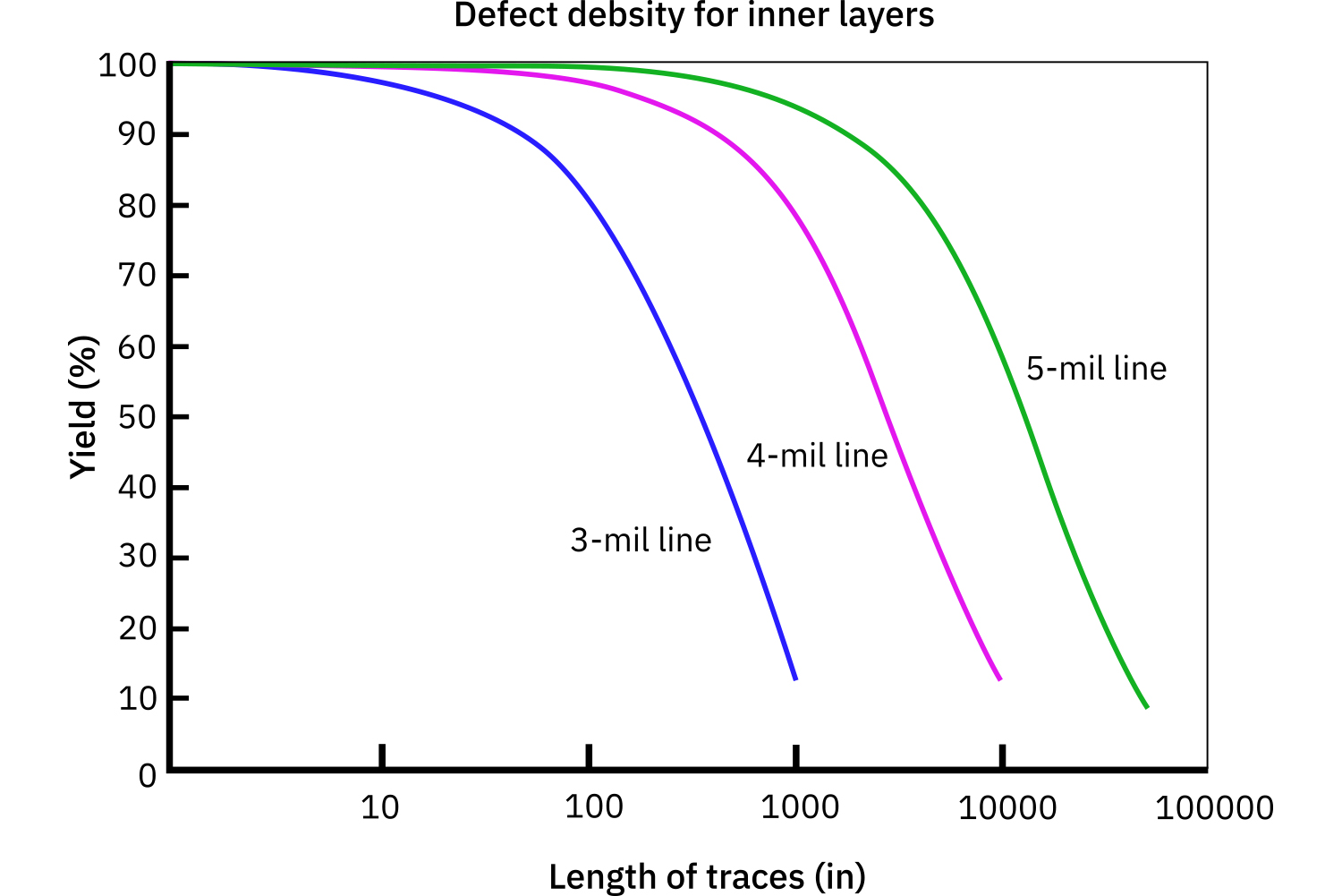
Because process yield influence the the cost of connectivity substrates. Therefore, knowing production yields is important for choosing the most cheap preparation method.
When there isn't enough room on existing layers to arrange all connected paths, the simplest and clearest solution is to simply add a layer. Because it has historically been a widely employed tactic.
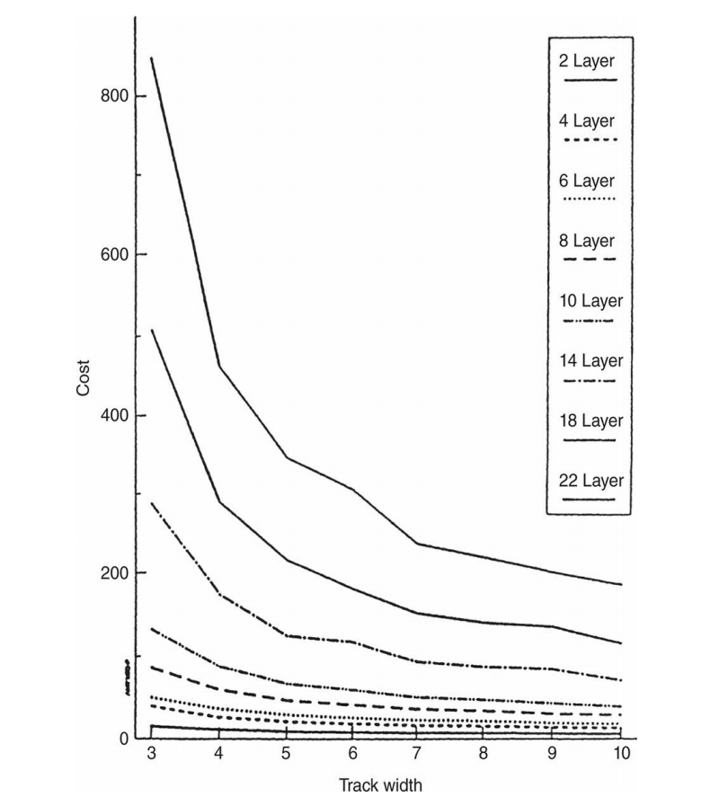
The designer should design careful research when he needs lower cost and lower layer counts in MLBs. Because the expense of adding a layer to a board increases. It is now obvious that the cost of a board and the number of layers are almost related. For instance, 6-in. x 8-in. MLBs produced in bulk with constant yields and density.
When the number of layers is increased in any of the line widths then designing yields reduce clearly. This happens quite while making circuit boards since MLB with more layers has more problems.
The engineers show the cost connection between the number of layers' widths by this image. Further, they give an example of how the finished MLB yield is impacted by layer count.
High-density interconnections are a key feature in the design of PCBs and PWBs. They allow for high-density circuits to be completed, while also offering a means of routing signals between various parts of the board. High-density interconnections are typically made of metal and offer many benefits over standard wire bonds.
And this article explains everything related to high-density interconnects and their role in PCBs and PWBs in detail. If you still have any questions, please feel free to contact us. We will approach you as soon as our team find time. Happy reading!
Still, need help? Contact Us: support@nextpcb.com
Need a PCB or PCBA quote? Quote now


 Surface

