
 Surface


Zhang

 NextPCB Capabilities
Printed Circuit Boards
NextPCB Capabilities
Printed Circuit Boards
 PCB Assembly
 Layer Buildup
 SMD-Stencils
 PCB Design-Aid & Layout
 Mechanics
 Quality
 Drills & Throughplating
 Factory & Certificate
 PCB Assembly Factory Show
Certificate
PCB Assembly Factory Show
Certificate
Support Team
Feedback:
support@nextpcb.com


An SMT stencil is a thin, precision-engineered sheet, typically made of stainless steel, featuring laser-cut holes (apertures) that align precisely with the component pads on the Printed Circuit Board (PCB). Its primary purpose is to transfer a precise, consistent, and uniform volume of solder paste or glue onto the designated pad locations on the bare board. The final deposited solder paste volume is determined entirely by the stencil's thickness and the dimensions of its apertures.
As HDI board layer counts increase and fine-pitch components (such as BGA) are applied, minor errors in the printing stage have an amplified effect on the final product quality. Therefore, seeking the highest precision stencil technology—the laser stencil—has become a key strategy for manufacturing high-reliability, complex PCBs.
The Laser Stencil gets its name from its unique manufacturing process: it is created by a high-precision laser ablation process that cuts the openings (apertures) into a thin stainless steel sheet.
Superior Cutting Quality: Laser cutting uses focused, high-intensity thermal energy to melt or vaporize the material, ensuring the precision of the cuts and the cleanliness of the edges, thereby eliminating material stress or potential chemical inconsistencies inherent in traditional chemical etching methods. This non-contact process achieves maximally burr-free cutting results and ensures optimal precision in positioning the openings. Burrs or rough edges create friction points that impede paste release, a major source of insufficient solder defects in fine-pitch assembly. Laser cutting significantly reduces this source of physical defects.
Tolerance and Capability: Modern laser systems can provide extremely high pad position accuracy, typically reaching a tolerance of (±25μm). This micron-level precision is essential for reliably printing 0.5mm to 0.4mm pitch components and small components like 0201 chip packages.
> Recommend reading: PCB Assembly Services: Market Size, Share, Trends, and Forecast
Table of Contents
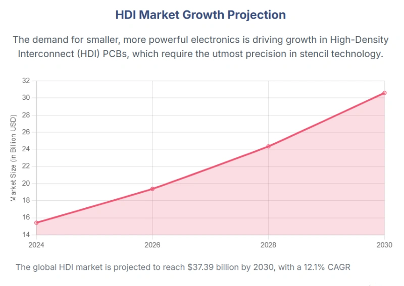
Current electronic product design is moving irreversibly toward lighter, thinner, and more compact devices. This trend has significantly boosted the High-Density Interconnect (HDI) PCB market. According to industry analysis and forecasts, the global HDI market size is expected to grow at a Compound Annual Growth Rate (CAGR) of 8.6% to reach approximately $16.9 billion USD by 2030. To achieve this, board layer counts are increasing (reaching up to 16-20 layers in high-end applications), and the widespread adoption of fine-pitch components (with pin pitches smaller than 0.5mm) is mandatory.
The Future is Smart: IoT and Market Growth
PCB assembly is aggressively moving into the ultra-fine pitch domain, with 0.4mm pitch connectors, Chip Scale Packages (CSP), and micro Ball Grid Arrays (micro BGA) becoming commonplace. Leading manufacturers like NextPCB focus on stable assembly capabilities for 0.35mm BGA and 01005 components, demonstrating the industry's pursuit of cutting-edge technology.
> Recommend reading: NextPCB SMT Assembly Capabilities Explained
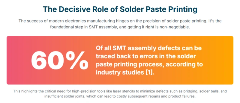
The solder paste application step in the Surface Mount Technology assembly process is notoriously error-prone. Studies show that up to 60% of potential SMT assembly defects can be traced back to solder paste printing issues. As tolerances shrink dramatically, minor variations in solder paste volume—whether excess paste causing shorts (bridging) or insufficient paste leading to unreliable connections—can directly result in costly assembly failures.
Therefore, the SMT stencil (or template) is no longer a simple tool, but the core mold for precise solder paste volume control.
Speed and Delivery Time: Compared to multi-step chemical processing, laser stencil production is simpler and faster, significantly shortening delivery times. Fast stencil delivery is crucial in rapid prototyping and high-mix, low-volume production environments, where slow stencil fabrication can bottleneck the entire PCBA process. Laser cutting technology combines high precision with rapid manufacturing capability, effectively reducing lead times.
Ease of Use and Cost Balance: Laser stencils are easy for operators to use and offer a good balance of high performance and moderate cost, making them affordable compared to highly specialized (and expensive) electroforming methods.
Post-Processing Enhancement: The quality and effect of laser stencils are further enhanced through post-processing treatments such as electroplating or electropolishing. These treatments optimize the aperture walls to achieve superior solder paste release characteristics.
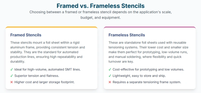
Stencils are categorized into framed and frameless types based on their use:
Framed Stencils: These are heavier and larger, designed for automatic and semi-automatic stencil printers, providing the necessary tension for consistent, high-volume printing. NextPCB offers various frame sizes to accommodate different printer models.
Non-Frame Stencils: These are lighter and smaller, primarily used for manual soldering or in low-volume or prototyping environments with specialized tensioning systems. Non-frame stencils offer a unique advantage in rapid prototyping because they are lightweight, simple to ship, and require minimal storage space when not in use. Non-frame stencil dimensions are customized based on customer demands, and their smaller size simplifies transportation, making them particularly convenient for quick proofing.
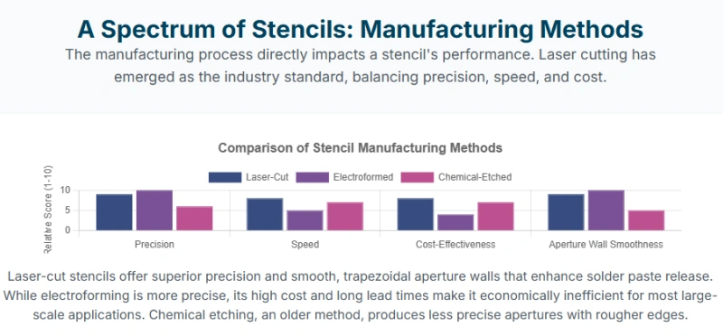
The precision requirements of modern PCB assembly have led to three main manufacturing technologies for SMT stencils: chemical etching, laser cutting, and electroforming. For the vast majority of modern high-density applications, laser cutting provides the optimal balance of performance and cost.
Etching Limitations: Chemical etching involves selectively dissolving exposed metal areas using corrosive solutions (typically acid). While chemical etching is lower cost for simple designs with larger pitches (greater than 0.63mm), this process leaves behind rougher edges and results in wider tolerance ranges (often ±50μm or more).
Quality and Environmental Considerations: The reliance on toxic chemicals in the etching process raises significant environmental concerns. More importantly, rough aperture walls tend to trap solder paste, leading to inconsistent deposits, bridging, and lower yield in fine-pitch scenarios.
Laser Technology Advantage: Laser cutting offers superior wall smoothness and aperture consistency, making it the clear performance winner for applications with pitches smaller than 0.5mm. The core value of laser stencils lies in their optimized throughput and yield, delivering the necessary precision for 0402 components at a reasonable cost and speed.
Electroforming Characteristics: Electroforming creates nickel stencils through an atom-by-atom growth process, achieving the highest precision, best repeatability, and extremely smooth aperture walls. This makes it the traditional choice for Absolute Ultra-Fine Pitch (UFP) applications, especially where extremely low area ratios are required.
Electroforming Drawbacks: The complex atom-by-atom growth process of electroforming results in the longest production cycle and the highest cost. This renders electroforming stencils economically inefficient in high-volume mass production. Additionally, there are practical limits to the thickness of electroformed stencils.
Closing the Gap: Although electroformed stencils possess inherently smoother walls, post-processing techniques applied to laser-cut stainless steel stencils, particularly nano-coating, have significantly narrowed the performance gap between the two technologies in terms of paste transfer efficiency. However, in extreme scenarios requiring Absolute Ultra-Fine Pitch (UFP) and extremely low Area Ratios, electroforming stencils remain the first choice due to their ultimate precision and smoothness, representing a performance limit laser technology struggles to match. Laser stencils maintain a significant advantage in production speed and controlled cost, making them the strategic choice in high-density manufacturing.
High-performance laser stencils combined with advanced coatings can achieve print quality comparable to electroformed stencils at a fast production speed and controlled cost, making electroformed stencils economically inefficient for most large-scale production applications.
| Aspect | Chemical Etching | Laser Cutting (Stainless Steel) | Electroforming (Nickel) |
|---|---|---|---|
| Precision Tolerance | ±50μm or greater (±50μm) | ±25μm Typical | ±15μm (Best Repeatability/Accuracy) |
| Fine Pitch Suitability | Limited (Best for >0.63mm pitch) | Excellent (Capable of 0.3mm pitch) | Superior (Ideal for Ultra-Fine Pitch) |
| Aperture Walls | Rougher Edges (High Paste Retention Risk) | Smooth (Can be enhanced by electropolishing) | Very Smooth (Minimum Adhesion) |
| Production Speed | Slower (Multi-step chemical process) | Fast (Simple and quick production process) | Longest Production Cycle |
| Cost | Lowest (For simple designs) | Medium to High | Highest |
| Environmental Impact | High (Requires handling toxic chemicals) | Low (Clean, non-contact process) | Moderate |
Learn PCB Assembly Services at NextPCB
The successful application of solder paste relies on the physical interaction between the solder paste, the stencil walls, and the PCB pad. Adherence to industry standards (specifically IPC-7525) is crucial for achieving repeatable high yield.
> Recommend reading: Circuit Board Solder: Types, Temperatures & How to Choose (Reflow & Hand Soldering Tips)
Balancing Principle: The stencil thickness must be carefully selected to deposit the correct volume of solder paste. When selecting the thickness, priority should be given to the smallest or most complex components (such as BGAs or fine-pitch QFNs).
Pitch and Thickness Examples: For components like 0.4mm pitch QFP, a thickness of 100μm is often required. For standard 0.5mm pitch QFP or larger BGA components (0.8mm pitch), a thickness of 120μm or 130μm may be used.
Stepped Stencil Application: For mixed-technology boards where large-volume components (such as SMT connectors, potentially requiring 150μm paste height) are mixed with tiny components (such as 0201 chips, requiring 100μm), a Stepped Stencil must be used. This involves selectively reducing (step-down) or increasing (step-up) the thickness in local areas to ensure every component receives its required solder paste volume.
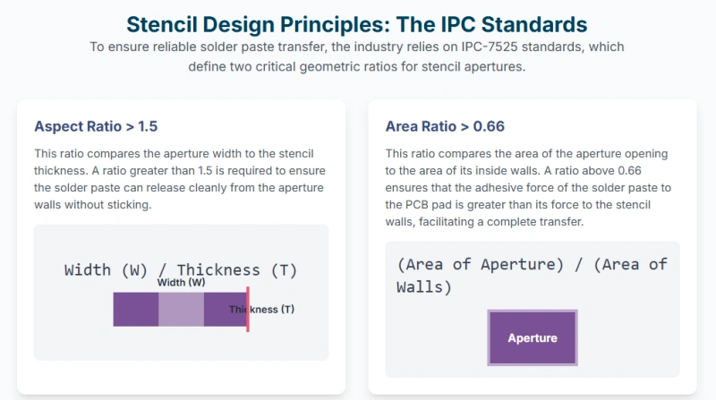
The IPC 7525 standard uses two key ratios to predict whether solder paste transfer will be complete and consistent. These ratios affect the uniform transfer of solder paste within the stencil aperture:
Aspect Ratio (AR): Defined as aperture width (W) / stencil thickness (T). This ratio relates to the squeegee's ability to push paste into the aperture without causing a "scooping" phenomenon.
Area Ratio (ARa): Defined as aperture surface area / aperture wall surface area( (L×W)/(2×(L+W)×T) ). This is the most critical metric, representing the balance of forces: the adhesion force between the paste and the stencil wall versus the cohesive/adhesive force of the paste connecting to the pad.
| Ratio Parameter | Definition | Leaded Solder Paste (Min. Recommended) | Lead-Free Solder Paste (Min. Recommended) |
|---|---|---|---|
| Aspect Ratio (W/T) | Aperture Width / Stencil Thickness | 1.5 | 1.5 |
| Area Ratio (A/W_area) | Aperture Surface Area / Aperture Wall Surface Area | 0.66 | 0.71 |
Area Ratio Physical Constraints: Since lead-free solder requires a higher Area Ratio (0.71 vs 0.66), this places extreme mechanical stress on stencil design. For aggressive fine-pitch designs, the aperture width (W) is fixed, and the stencil thickness (T) must be reduced to meet the ratio requirement. When cutting-edge component designs inevitably result in extremely low Area Ratios (e.g., <0.5), traditional printing processes will fail. Achieving high-yield printing requires chemical modification of the stencil surface to overcome the physical limits of adhesion.
Aperture Reduction: Stencil aperture sizes should typically be slightly smaller (5-10%) than the PCB pad size to prevent excess solder paste from squeezing out, which causes bridging.
Trapezoidal Apertures: Laser cutting allows for the creation of modified aperture shapes. Trapezoidal apertures are critical because they feature a wider opening on the squeegee side, tapering slightly (3-5 degrees) toward the PCB side. This geometry reduces the surface area of the solder paste sticking to the stencil wall, thus enhancing the solid release characteristics of the solder paste and improving deposition consistency.
To push beyond IPC minimum limits and meet the demands of 0.3mm pitch, modern laser stencils are enhanced through specialized surface treatments and structural modifications.
Mechanism of Action: Nano-coating involves the uniform application of an extremely thin (20-100nm thick) fluorosilicone polymer layer onto the stencil foil surface and the critical aperture walls, often via high-vacuum deposition technology. This creates a highly hydrophobic and oleophobic (non-stick) surface.
Nano-Coated Laser Stencil vs. Electroforming: Nano-coated laser stencils have been shown to provide cleaner printing after long cycles without wiping compared to uncoated electroformed stencils. This suggests that surface treatments applied to laser-cut foils can often surpass the inherent smoothness advantage of bare electroformed stencils in terms of paste release performance and defect reduction. The performance boost brought by nano-coating makes laser cutting a more economically efficient and strategic choice than traditional electroforming for high-volume manufacturing.
Mixed Design Necessity: Stepped stencils, featuring variations in thickness, are essential for boards that combine large-volume components (such as connectors or RF shields requiring higher paste volume) with ultra-fine pitch components.
Implementation: NextPCB utilizes laser processing capability to manufacture precise step-down regions (thinner foil) for fine-pitch components (e.g., 100μm for 0.4mm pitch), and step-up regions (thicker foil, often achieved through local deposition) for larger components (e.g., 150μm for ceramic BGAs). This ensures that every component receives the exact required volume of solder paste during the same printing process, achieving optimal soldering reliability.
NextPCB's advanced SMT capabilities rely directly on the deployment of high-precision laser stencil technology and stringent quality control.
Ultra-Fine Pitch Assembly: NextPCB's SMT production lines are optimized for fine-pitch component placement, guaranteeing stable assembly for challenging components like 0.35mm pitch BGA and 01005 components. Achieving this performance mandates the use of laser stencils with micron-level positioning accuracy (≤±25μm) and optimized paste release characteristics (achieved through advanced coatings and trapezoidal apertures).
High Reliability Standards: NextPCB adheres to IPC Class 3 quality standards for assembly and offers manufacturing processes certified by the highest standards in the automotive and medical industries. This commitment to reliability requires the mandatory use of high-precision laser-cut stencils to ensure the consistency of solder joint integrity.
Mandatory Inspection: The superior deposition accuracy achieved by laser stencils is verified through mandatory inspection methods, including automated X-ray inspection (AXI) for complex packages like BGAs. This quality control step verifies that the deposited paste volume precisely matches the design specification before reflow soldering, reducing costly subsequent rework. The combination of high-precision laser stencils and mandatory X-ray inspection is a powerful risk mitigation strategy.
One-Stop Solution: As a full-service PCBA provider, NextPCB integrates laser stencil fabrication directly into its one-stop process. The company offers DFM/DFA (Design for Manufacturability/Assembly) review services, automatically optimizing aperture size and stencil thickness to maximize printability before manufacturing begins. This technical expertise minimizes the design risks associated with complex fine-pitch components.
NextPCB's capability to handle 0.35mm BGA components confirms its adoption of best-in-class stencil fabrication and process control. This component pitch directly demands ≤±25μm tolerance accuracy from the stencil, ruling out low-cost alternatives (like etching). Given the high cost of high-density boards, ensuring initial print accuracy via laser stencils, and using X-ray inspection as a crucial gate, captures defects before component placement and soldering, strongly safeguarding overall PCBA yield.
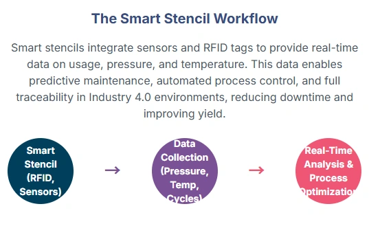
Laser stencil technology is rapidly moving beyond simple mechanical cutting toward smart, data-driven systems integrated into the Industry 4.0 environment.
Data-Driven Optimization: Artificial Intelligence (AI) and Machine Learning algorithms are increasingly used to monitor and analyze SMT production data in real time. This enables the automatic optimization of printing parameters (e.g., squeegee speed, pressure) and predictive defect modeling.
AI-Driven Stencil Design: Future advancements include leveraging AI-powered PCB stencil design software to automatically optimize the aperture size and geometry (e.g., trapezoidal cuts, aperture reduction) for every single pad on a specific PCB design, thus automatically maximizing the Area Ratio and ensuring optimal paste volume.
Impact: AI integration enhances efficiency, shortens time-to-market, and minimizes human errors, supporting the manufacturing industry's transition toward smarter, greener production.
> Recommend reading: Building Better PCBs: Key Design Strategies and Modern Manufacturing Tips
Real-Time Monitoring and Data Feedback: Innovations like Smart Stencils integrate sensors (for pressure and temperature) and RFID tags directly into the frame. This integration provides real-time data feedback during the printing process, helping operators optimize parameters like squeegee pressure and speed.
Service Life and Efficiency Management: By using RFID tags to record every print cycle, smart stencils prevent the accidental use of outdated or expired stencils, even when moved between different lines. They provide real-time inventory and usage data, and support critical maintenance and replacement scheduling by seamlessly integrating with MES/ERP systems for accurate tracking and efficient material handling (e.g., Pick-to-Light technology). Real-time data analysis and remote monitoring significantly enhance the overall efficiency of the production line and reduce downtime caused by manual checks or end-of-life stencil usage.
> Recommend reading: SMT Stencil: The Ultimate Guide Is Here
While laser cutting remains the primary method for foil fabrication, the future may see the use of Additive Manufacturing (3D Printing) technology to deposit solder paste directly onto the PCB, potentially eliminating the need for physical stencils. Furthermore, 3D printing can also be used to create custom stencils with geometries that are unachievable through subtractive (laser) methods, further increasing precision and consistency for complex components.
Laser stencil technology has become the cornerstone of modern high-density PCB assembly. Its micron-level precision (±25μm) and rapid manufacturing capability strike an optimal balance between performance and cost, making it especially suitable for 0.5mm to 0.3mm fine-pitch components.
> Recommend reading: PCB Assembly Services: Market Size, Share, Trends, and Forecast
Key Takeaways:
NextPCB, complemented by IPC Class 3 standards and mandatory X-ray inspection, ensures its leading position in ultra-fine pitch PCBA services, providing a highly reliable solution for the electronics industry to meet the challenges of more complex and precise miniaturized designs.

Still, need help? Contact Us: support@nextpcb.com
Need a PCB or PCBA quote? Quote now

