

 NextPCB Capabilities
 PCB Assembly
 Layer Buildup
 SMD-Stencils
 PCB Design-Aid & Layout
 Mechanics
 Surface
 Quality
 Drills & Throughplating
 Factory & Certificate


Introduction:
As billions of connected devices come online, the pressure to turn ideas into reliable products has never been higher. Recent estimates count 18.8B connected IoT devices and rising, while cellular IoT alone is projected to exceed 7B connections by 2030—a scale that rewards teams who can prototype, validate, and ship fast without compromising quality.
In hardware, late fixes are brutally expensive. That's why world-class teams "shift left" and use stage-gates like EVT → DVT → PVT to push risk discovery earlier—where a defect can cost orders of magnitude less to resolve than in the field.
This guide distills a practical playbook for IoT prototyping hardware: when to choose MCUs/SBCs, where SoMs + carrier boards accelerate time-to-market, and how DFX/DFM/DFT and agile habits turn one-off demos into production-ready designs. By combining rapid iteration with manufacturability, testability, and smart supply decisions, you can cross the dev-board to custom PCB valley faster—and launch with confidence.
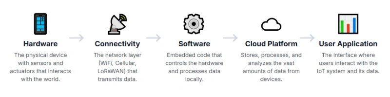
Table of Content:
- Part I: The Strategic Foundation of IoT Prototyping
- Part II: The Critical Transition from Prototype to Production
- Part III: A Professional's Blueprint: Custom PCB Best Practices
- Part IV: From Lab to Market: The Real-World Journey
- Conclusion: Realizing Your IoT Vision
Part I: The Strategic Foundation of IoT Prototyping
1. The Bridge from Concept to Reality: Why IoT Prototyping is Crucial
The Internet of Things (IoT) is changing the world at a stunning pace, from the convenience of smart homes to the efficiency gains of industrial automation. However, turning an IoT idea from a blueprint into reality is far from simple. It involves a complex ecosystem of interconnected hardware, firmware, software, and the cloud, where a misstep in any single area can lead to project failure.
For this reason, a strategic approach to hardware prototyping is the critical first step to de-risking a project and ensuring its technical and commercial viability.
Prototyping is the process of rapidly creating an early looks-like and/or works-like version of a proposed IoT solution. Its core objective is to evaluate a device or system's feasibility, functionality, and usability before committing to large-scale production.
This stage helps development teams identify problems, find optimal solutions, discard unsuitable ideas, and pinpoint potential technical challenges early on. Unlike software development, errors in hardware can be catastrophic. Once a project reaches later stages, a hardware flaw not only wastes time but also squanders valuable physical materials and immense capital investment.
Therefore, deep investment in prototyping during the early stages should not be seen as a cost, but as a crucial risk mitigation strategy. The entire product development lifecycle, from concepting to Engineering Validation Testing (EVT) and Design Validation Testing (DVT), is designed to minimize this risk at every turn.
2. The Agile Hardware Mindset: The Power of Rapid Iteration
Modern hardware development has adopted agile methodologies from software development to accelerate development cycles and optimize outcomes. In the past, hardware design often followed a rigid waterfall model: the hardware team completed its design, handed it off to the firmware team, and so on. However, IoT is a system of systems, and this linear approach is highly prone to failure. If hardware engineers design a board without fully considering firmware needs or cloud platform requirements, severe integration issues are likely to emerge late in the project.
The core of the agile approach is delivering a Minimum Viable Product (MVP) in short, iterative cycles. This method requires hardware, software, data science, and design teams to communicate seamlessly and work in parallel. By parallelizing workflows, teams can identify integration problems immediately rather than months down the line.
This collaborative approach directly led to the concept of atomic work, which involves breaking a complex system into independent, testable, and minimal units. For example, instead of reviewing an entire complex circuit board at once, it is broken down into more manageable modules like the power supply, Microcontroller Unit (MCU), memory, and sensor layout. This decomposition allows for continuous and early testing and remediation, which significantly lowers the overall project risk.
3. The Prototyping Toolbox: Selecting Core Hardware
Choosing the right prototyping hardware is critical to a project's success. There are a variety of core hardware options on the market, each with its unique advantages.
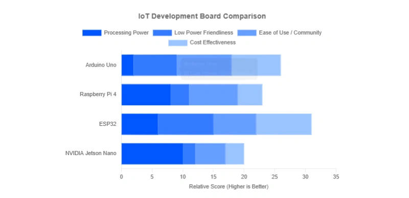
Microcontrollers (MCUs) and Single-Board Computers (SBCs):
These hardware options involve a trade-off between power consumption and computing power. For instance, while the Raspberry Pi is easy to use, its high power consumption makes it unsuitable for low-power, battery-operated devices. Experts select more power-efficient MCUs like the Nordic nRF52 or ESP32 based on project requirements.
Sensors and Actuators:
The core of an IoT device is to collect environmental data via sensors and use actuators to respond to changes. From smart thermostats to industrial sensors, every application has specific sensor needs. The table below lists several common IoT sensors and their real-world applications, demonstrating the breadth and diversity of this field.
|
Sensor Type |
Functional Description |
Examples of Typical Applications |
|
Temperature Sensor |
Measures the temperature of an environment or object to ensure it is within a safe or optimal range. |
Preventing boiler overheating; monitoring temperature conditions during food and beverage transport; smart thermostats; smart baby monitors. |
|
Humidity Sensor |
Measures the moisture content in the air to maintain a comfortable and safe environment. |
Product quality control in the food and pharmaceutical industries; maintaining safe working environments on factory floors; smart baby monitors. |
|
Pressure Sensor |
Monitors the pressure of gases and liquids to detect anomalies. |
Monitoring liquid levels in water treatment facilities to prevent overflow; industrial process control. |
|
Accelerometer/Gyroscope |
Measures the vibration, motion, and orientation of an object. |
Predictive maintenance of industrial equipment by detecting abnormal vibrations before failure occurs; smartwatches and fitness trackers; drone or robot navigation. |
|
Gas Sensor |
Detects gases or toxic substances in the air. |
Detecting gas leaks in industrial environments; maintaining employee health in factories; fire and safety detection equipment. |
|
Infrared Sensor |
Senses the environment by emitting and detecting infrared radiation, used for counting, alarms, or remote control. |
Item counting; burglar alarms; radiation thermometers. |
|
Proximity Sensor |
Detects whether an object has entered a predefined area or distance without physical contact. |
Item detection on assembly lines; robot collision avoidance. |
|
Optical Sensor |
Senses light and can be used to identify external factors like temperature, lighting, and voltage. |
Smart lighting systems; monitoring plant health in smart agriculture. |
A project's success often stems from a deep understanding and correct selection of these foundational components. IoT is a field that requires tailored solutions for specific needs, which naturally leads to the demand for custom Printed Circuit Board services.
Part II: The Critical Transition from Prototype to Production
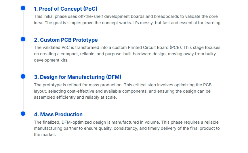
1. The Prototyping Bottleneck: Why Dev Boards Are Not Enough for Mass Production
Development boards are an indispensable tool during the early stages of an IoT project's lifecycle. They provide out-of-the-box functionality at a low initial cost, making them ideal for Proof of Concept (PoC) and rapid prototyping. However, for any product aimed at scalability, development boards have inherent limitations that make them unsuitable for mass production.
Dev boards are not designed for large-scale manufacturing; their primary limitations include:
The transition from a dev board to a custom PCB is a death valley for many hardware startups, as the two design philosophies are fundamentally different.
Dev boards prioritize ease of use, while custom PCBs aim for manufacturability, low unit cost, specific form factor, and robustness. If a team fails to understand this transition, it can waste a significant amount of time and money in the later stages.
A case from Reddit exemplifies this: a developer who received positive feedback on their prototype later transitioned to a custom PCB, but the first three versions were a mess due to power management and RF interference issues. This highlights that features working well on a dev board can fail completely in a custom design due to unoptimized layout and component selection.
Although custom PCBs have a higher initial cost, they are often the more cost-effective choice in the long run for projects with annual production volumes exceeding a few hundred units.
2. The Smart Transition: From Dev Board to Production-Ready Design
The path from prototype to production isn't just a binary choice between a dev board and a fully custom PCB. Modern hardware development has introduced a powerful intermediate solution: the System on Module (SoM). An SoM is a miniature circuit board that integrates complex functions like a processor, memory, and high-speed interfaces, acting as the system's brain.
SoM + Carrier Board Architecture:
An SoM is typically used with a custom-designed carrier board to form a complete system. The SoM handles the complex computing tasks, while the custom carrier board provides application-specific peripherals (e.g., GPIO, camera interfaces), sensors, connectors, and power.
SoM's Advantages and Trade-offs:
For startups or small teams, designing a complete chip-down custom board requires specialized RF engineers and a significant amount of time. The SoM approach allows them to focus on their core value—their unique application and custom carrier board—thus dramatically accelerating the time-to-market. This is a strategic decision that demonstrates a deep understanding of the entire product development process.
|
Feature |
Dev Board |
System on Module (SoM) |
Custom PCB (Chip-down) |
|
Initial Cost |
Lower |
Medium |
Higher |
|
Unit Cost (at scale) |
Higher ($10-$40+) |
Medium |
Lower |
|
Time to Market |
Extremely Fast (days) |
Fast (months) |
Longer (6+ months) |
|
Design Flexibility |
Limited |
High (via carrier board) |
Extremely High |
|
Design Complexity |
Very Low (plug-and-play) |
Medium (carrier board design) |
Extremely High (requires professional RF engineers) |
|
Mass Production Suitability |
Very Low |
Suitable for low- to mid-volume |
Suitable for mass production |
|
Typical User |
Hobbyists, beginners |
Companies focused on applications, low- to mid-volume products |
High-volume product companies with dedicated hardware teams |
This table provides a clear comparison to help innovators make informed strategic decisions
based on their project's unique needs, volume goals, and team expertise.
Part III: A Professional's Blueprint: Custom PCB Best Practices

1. The Three Pillars of IoT PCB Design
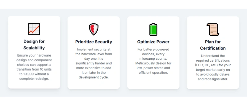
Custom PCB design is a precise art of balancing power efficiency, size, and connectivity. These three pillars are not independent but often constrain each other.
These three pillars are not isolated; they are often in conflict. For example, miniaturizing a board can make thermal management more difficult by reducing the surface area for heat dissipation. A smaller board also presents challenges for RF design, as a smaller ground plane can impact signal integrity. A professional's value lies in balancing these trade-offs to ensure the design is not only theoretically sound but also robust and reliable in production.
2. Design for Excellence (DFX): The Path to a Flawless Launch
Design for Excellence (DFX) is a comprehensive engineering philosophy that encompasses Design for Manufacturability (DFM), Design for Assembly (DFA), and Design for Testability (DFT), among other aspects. Incorporating DFX principles into the design is key to a successful product launch and scalability.
These three (DFM, DFA, DFT) form the foundation of DFX. They are not unnecessary hassles but crucial risk mitigation activities that ultimately accelerate the entire project timeline. A top-tier manufacturing partner leverages expertise in these areas to help innovators turn these principles into reality.
|
DFX Principle |
Core Objective |
Action List (including but not limited to) |
|
DFM (Manufacturability) |
Ensure the design is easy, efficient, and cost-effective to produce, avoiding production failures and material waste. |
Collaborate with your manufacturer early to get design feedback; optimize component layout and trace spacing; design a proper PCB stack-up, especially for RF circuits. |
|
DFA (Assembly) |
Simplify the assembly process, reducing labor costs and error rates. |
Reduce the number of parts and combine functions; use standardized, easy-to-place components for automated pick-and-place machines; design parts with self-locating and self-fastening features (like snap-fits). |
|
DFT (Testability) |
Add testing capabilities to the design for manufacturing testing and diagnostics. |
Place test points or headers on key nodes for easy probing; design isolated modules that can be tested independently; incorporate diagnostic modes in firmware to isolate functions. |
Part IV: From Lab to Market: The Real-World Journey
1. Case Studies: Lessons from the Real World
The journey of a successful product always validates the principles discussed above. Here are some real-world examples from various sectors that illustrate the complete path from prototype to global product.
> Recommend reading: KiCad 9: Design & assemble an ESP32 IoT 4-layer PCB
These case studies collectively prove that the principles discussed in this article are not theoretical. They are the foundation of successful real-world products and emphasize that a successful IoT product is not just about the hardware but also about the entire ecosystem—including software, security, and the overall business model.
2. Your Innovation Partner: How NextPCB Accelerates Your Journey
From concept to a global product, the IoT development journey is full of challenges. For an innovator, juggling product design, software development, marketing, and financing can be an overwhelming task. This is where a professional, integrated manufacturing partner becomes invaluable.
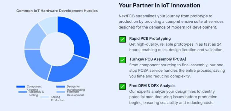
NextPCB is a strategic partner that provides innovators with a one-stop shop for product realization, from prototyping to mass production. With over 15 years of experience in manufacturing hardware products, its core value is helping clients minimize time spent in 'Death Valley'. Through its proven methodology and deep supply chain, NextPCB provides a consistent, repeatable, and efficient New Product Introduction (NPI) process that helps innovators turn ideas into great, global products. NextPCB's services include:
A top-tier manufacturing partner is not just a service provider; it's a strategic asset for a project. Entrusting the complexities of supply chain and manufacturing to NextPCB allows your team to focus on innovation itself, gaining a crucial first-mover advantage in a competitive market.
> Recommend reading: PCBs Power Electronic Devices: Wearables, IoT & Smart Homes
Conclusion: Realizing Your IoT Vision
Turning an IoT concept into a global product is a complex journey, but it is not insurmountable. The key to success is adopting a strategic approach from the start and embracing a mindset of continuous iteration and optimization.
Take the next step:
- Get an instant PCB quote
- Request a PCB assembly quote
- Run a free online DFM/Gerber check
- Talk to an engineer
Ultimately, IoT prototyping hardware is more than just a set of tools; it is the blueprint for your vision and the bridge that transforms a digital idea into a physical reality. With wise decisions and a professional partner, any innovator has the capability to take an idea from the lab to the global market and achieve success in the age of IoT.
> Recommend reading: PCB Antenna Layout & Keep-out Design: Best Practices for IoT Hardware


