

 NextPCB Capabilities
 PCB Assembly
 Layer Buildup
 SMD-Stencils
 PCB Design-Aid & Layout
 Mechanics
 Surface
 Quality
 Drills & Throughplating
 Factory & Certificate


Introduction
In electronic products, thermal design is not just about adding a heatsink. It is a system-level task grounded in three mechanisms: conduction, radiation, and convection. For package- and board-level thermal characterization, the industry commonly relies on the JEDEC JESD51 family (e.g., θJA, ΨJT) to obtain comparable thermal metrics; at the PCB design level, IPC-2221 provides generic design guidance that includes thermal considerations. Together, these frameworks give a common language to discuss heat paths, estimate junction temperature, and optimize board structures early in design to keep thermal risk within predictable bounds.
> Recommend reading:
- PCB Thermal Design Basics (1): Substrate Material Selection
- PCB Thermal Design Basics (2): Component Layout
- PCB Thermal Design Basics (3): PCB Wiring Layout
1. Three Modes of Heat Transfer in PCB Thermal Design
Whenever there is a temperature difference, heat flows. PCB and component cooling leverages three basic modes: conduction, radiation, and convection.
1.1 Conduction
The ability of a material to conduct heat is described by its thermal conductivity, k. In solids, conducted heat increases with k, effective cross-sectional area along the heat path, and temperature difference, and decreases with path length/material thickness. This is why design practice aims for short, wide, direct heat paths to reduce equivalent thermal resistance. Note that k is a material property but not strictly constant: it varies with temperature and depends on microstructure (e.g., electron transport in metals, molecular vibrations in polymers/resins). Therefore, evaluations should use data in the target operating temperature range, not a single room-temperature value.
> Recommend reading: PCB Thermal Design Case Study: Copper Thickness for Uniform Heat Load
In composites or layered stacks, conduction can be anisotropic (e.g., strong in-plane, weak through-thickness). In such cases, confirm effective conductivity along the dominant heat-flow direction and orient stack-ups/heatsinks to align with high-k axes. At interfaces, contact thermal resistance can dominate: even with high-k materials, poor filling, rough surfaces, or insufficient clamping trap heat at the joint. Hence appropriate TIMs, assembly pressure, and surface preparation are required to stabilize interface resistance and lot-to-lot consistency.
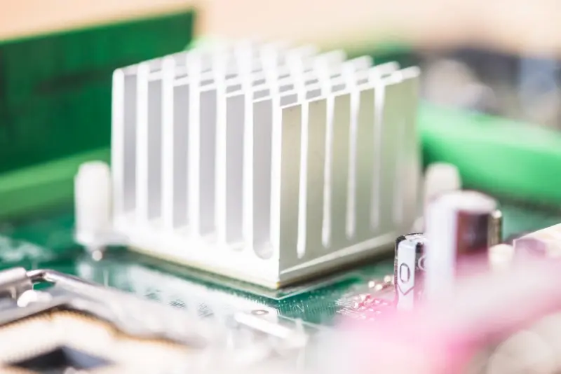
Following these principles, designs commonly use aluminum alloys or copper for heat spreaders/sinks; for high-power parts, thicker sinks or larger cross-sections shorten the heat path and reduce spreading resistance. With suitable TIMs and assembly processes, the intrinsic material conductivity translates into actual device temperature reduction.
Thermal conductivities from an IPC reference table:
|
Material |
Thermal Conductivity, k (W/m·°C) |
Thermal Conductivity, k (cal/(cm·s·°C)) |
|
Still air (at rest) |
0.0267 |
0.000066 |
|
Epoxy resin |
0.200 |
0.00047 |
|
Thermally conductive epoxy |
0.787 |
0.0019 |
|
Aluminum alloy 1100 |
222 |
0.530 |
|
Aluminum alloy 3003 |
192 |
0.459 |
|
Aluminum alloy 5052 |
139 |
0.331 |
|
Aluminum alloy 6061 |
172 |
0.410 |
|
Aluminum alloy 6063 |
192 |
0.459 |
|
Copper |
194 |
0.464 |
|
Low-carbon steel |
46.9 |
0.112 |
1.2 Radiation
Thermal radiation is heat transfer via electromagnetic waves (primarily infrared). Radiative power depends on a material's emissivity, the effective radiating area, and the object's thermal energy. With equal emissivity, rough, matte, or oxidized/coated surfaces radiate more strongly than bright, polished metal surfaces. For radiating surfaces, matte/dark finishes generally improve radiative heat loss. Closely spaced heat sources mutually absorb each other's radiation; increasing separation reduces this radiative coupling and mitigates thermal interaction between adjacent parts.
1.3 Convection
Convection is heat exchange in liquids or gases. Under quasi-steady conditions, the heat transfer rate is proportional to the temperature difference between the surface and the ambient. The engineering form (Newton’s law of cooling) is:
Q_e = h_c × A_s × (T_s − T_a)
where (Q_e) is the convective heat transfer rate, (h_c) the heat transfer coefficient, (A_s) the wetted surface area, (T_s) the surface temperature, and (T_a) the ambient temperature. This expresses “heat flux proportional to ΔT” for convection.
Importantly, (h_c) is not a constant; it varies with fluid properties (density, viscosity, thermal conductivity, specific heat), flow regime (laminar/turbulent), velocity and direction, surface geometry/roughness, and convection type (natural/forced). Turbulent mixing thins the boundary layer, so (h_c) tends to exceed that of laminar flow; forced convection (fans, pumps) typically yields larger (h_c) than natural convection. Practical ranges depend on medium and conditions and must be determined by correlations or tests for the geometry and flow in question.
Heat transfer coefficients in air:
|
Convection Mode |
Heat Transfer Coefficient ((h_c)) |
|
Natural convection |
0.0015 ~ 0.015 W/in²·°C |
|
Forced convection |
0.015 ~ 0.15 W/in²·°C |
The table illustrates how forced convection can substantially raise (h_c) and thus improve cooling capacity.
2. Effects of Temperature (High Temperature) on Components and Electronic Products
Rising temperature degrades performance and raises failure risk across device classes. Typical observations include: resistance drift in resistive parts; shortened lifetime of capacitors; decreased insulation performance in transformers/chokes; and, at solder joints, embrittlement, strength loss, and potential cracking/detachment.
For semiconductors, higher junction temperature increases gain and device current; without temperature compensation and effective heat paths, this can lead to thermal runaway and failure. Among many failure drivers, high temperature is often primary (others include vibration, humidity, and dust). Temperature and failure rate increase together; engineers commonly express this using the following relation for estimation:
F = A_c − E / (K · T)
where (F) is the failure rate, (A_c) a constant, (E) power, (K) Boltzmann’s constant, and (T) junction temperature. Reported experience indicates: every +2 °C reduces reliability by ~10%; with a 50 °C rise, service life can drop to 1/6 of that at 25 °C rise; and ~45% of electronic product failures are attributed to excessive temperature.
3. PCB Thermal Performance Analysis
During pcb fabrication, soldering, and testing, PCBs are repeatedly exposed to harsh conditions: e.g., 260 °C for 10 s during soldering, 288 °C for 2 min for lead-free processes, and temperature cycling between 125 °C and 65 °C in reliability tests. If the base material lacks sufficient heat resistance, these conditions reduce dimensional stability, inter-laminar adhesion, and planarity, and lower conductor peel strength at elevated temperature. Therefore, thermal impacts from processing/testing should be captured as design-time constraints.
In service, ambient variation combined with component/trace dissipation drives continuous temperature changes. The immediate cause of PCB temperature rise is power-dissipating components; different dissipations produce different heat strengths. Spatially and temporally, boards exhibit local hot spots vs. board-level rise, and short-term transients vs. long-term steady-state rise.
Insufficient thermal design often appears later as plated-through-hole (PTH) failure, solder joint cracking, or parameter drift after temperature cycling or shocks. Even if assemblies pass initial tests, inadequate heat removal during long operation can shift component temperature coefficients, alter operating points, and cause system malfunctions; with further accumulation, failures can escalate to device damage, solder joint fracture, PTH failure, or board warpage. Consequently, designs should perform targeted thermal analysis: identify sources and paths of temperature change, apply structural/process measures accordingly, lower peak temperature rise or narrow temperature swings, and keep thermo-mechanical effects within assembly and product specifications.
For PCB thermal analysis, evaluate power, board structure, installation environment, radiation, conduction, and convection under a consistent operating scenario:
- Electrical power — Provide power per unit area and a power map to locate hot spots and set boundaries for analysis.
- PCB structure — With board size and base material, judge in-plane/through-thickness spreading and potential bottlenecks.
- Installation & enclosure — Orientation (vertical/horizontal), enclosure sealing, and standoff to chassis define external heat-transfer boundaries.
- Radiation — Use surface emissivity with neighbor temperature differences and absolute levels to estimate radiative contribution.
- Conduction — Decide on heatsinks and assess additional conductive paths through structural parts; include interface quality/TIMs.
- Convection — Distinguish natural vs. forced convection and estimate their effects on heat removal.
These factors are coupled in a common thermal-resistance network and jointly determine temperature rise. Analyze them for the specific product and operating conditions to obtain estimates that match real hardware.
Conclusion
This overview organized PCB thermal design around conduction, radiation, and convection, using a material thermal-conductivity table, the engineering form of Newton's law of cooling (Q_e = h_c A_s (T_s - T_a)), and empirical temperature-reliability relations to build an entry-level framework. In practice, use JESD51 characterization methods and IPC-2221 board-level guidance as a shared basis, and close the loop in design with heat-path identification → capacity estimation → prototype verification → boundary checks.
Next reading: To connect thermal design with manufacturability and maintainability, continue with Basic Principles of PCB Design (layout, routing, vias/stack-up, impedance, EMC, DFM/DFT). These principles cross-check the thermal analysis items above and help converge on a robust system plan early.
Ready to validate your thermal choices on real hardware?
Prototype and scale with NextPCB: quick-turn PCB/PCBA, controlled-impedance and high-TG stackups, and engineering DFM checks that catch thermal bottlenecks before fab. Upload your Gerbers at NextPCB.com, or contact the team for a free preliminary review of stack-up, copper weight, and component heat-spreading strategy.


