

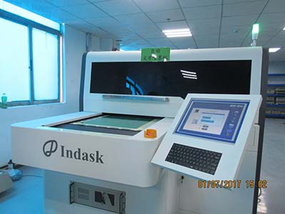
 NextPCB Capabilities
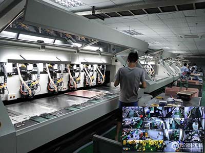
 PCB Assembly
 Layer Buildup
 SMD-Stencils
 PCB Design-Aid & Layout
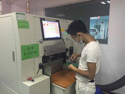
 Mechanics
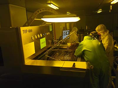
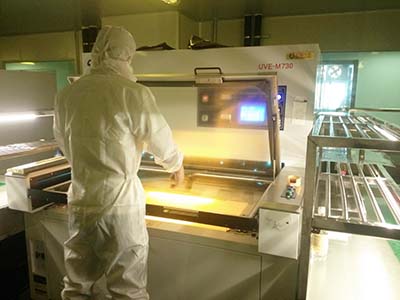
 Surface
 Quality
 Drills & Throughplating
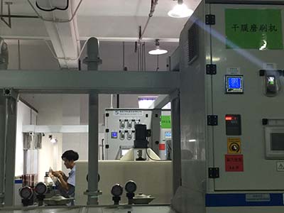
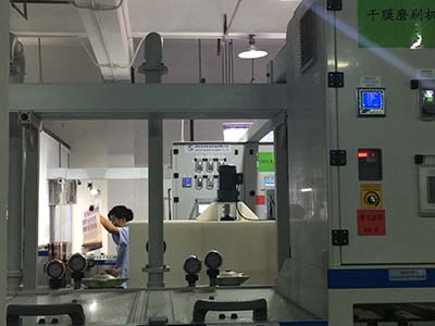
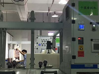
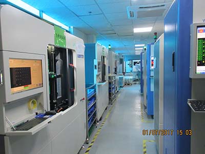
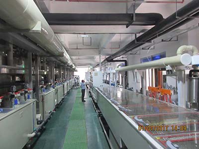
 Factory & Certificate


-
-
-
-
Two major problems in high speed PCB design
1. EMC, EMI. 2. Routing skills for high-speed differential signals
4195 1 0 Shares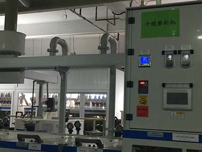
-

-
-
-
-
Method of avoiding transmission line effects
The ways to control the effects of transmission line effects from the following aspects.
4209 2 0 Shares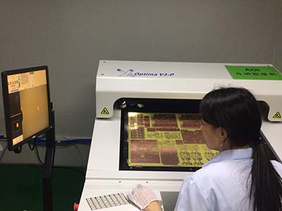
-
-
-
-
Analysis of problems in PCB design (16-25)
Can you introduce some foreign technical books and materials on high-speed PCB design?
4805 8 0 Shares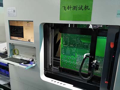
-
-
-
-
-
-
-
Categories
Recommended Article:
- IRLB3034 Pinout, Datasheet & Equivalents: The Complete Reference
- Raspberry Pi 5 Pinout: Full GPIO Reference & What RP1 Changes
- Raspberry Pi 4 Pinout: Full GPIO Reference & BCM2711 Details
- Raspberry Pi Pico GPIO Pinout: Complete Pin Reference & Peripheral Map
- Raspberry Pi GPIO Pinout: The Complete Guide (Pi 5, Pi 4 & Pico)
- 78H24 Pinout Explained: What It Really Is (and What to Use Instead)
- Rogers 5880 (RT/duroid 5880): Dielectric Constant & Datasheet Guide
- Circuit Boards China: PCB Fabrication Guide 2026
- 5-Band Resistor Color Code: How to Read It (Free Calculator Inside)
- What Is a Microvia? Types, Design Rules & HDI Guide