Support Team
Feedback:
support@nextpcb.com1. The structure of the multi-layer board:
In order to perform good impedance control on the PCB, we must first understand the structure of the PCB:
Generally speaking, the multi-layer board is made by laminating and laminating the core board and the prepreg. The core board is a hard, specific thickness, two-bread copper sheet, which is the basic material for the printed board. . The prepreg constitutes a so-called wetting layer which acts to bond the core sheet, although it also has a certain initial thickness, but its thickness will change somewhat during the pressing process.
Usually the outermost two dielectric layers of the multilayer board are both wetting layers, and a separate copper foil layer is used as the outer copper foil on the outside of the two layers. The original thickness specifications of the outer copper foil and the inner copper foil are generally 0.5OZ, 1OZ, 2OZ (1OZ is about 35um or 1.4mil), but after a series of surface treatments, the final thickness of the outer copper foil is generally Will increase by nearly 1OZ. The inner copper foil is the copper coated on both sides of the core board, and the final thickness is very small from the original thickness, but due to etching, a few um is generally reduced.
The outermost layer of the multilayer board is a solder mask, which is what we often call "green oil". Of course, it can also be yellow or other colors. The thickness of the solder mask is generally not easy to determine accurately. The area without copper foil on the surface is slightly thicker than the area with copper foil. However, because of the lack of thickness of copper foil, the copper foil is still more prominent when we use You can feel it when you touch the surface of the printed board with your fingers.
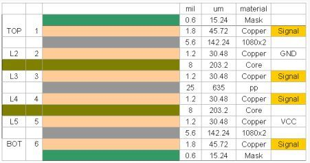
When making a printed board of a certain thickness, on the one hand, it is required to reasonably select the parameters of various materials. On the other hand, the final forming thickness of the prepreg is also smaller than the initial thickness. Below is a typical 6-layer laminate structure:
6-layer stack-up structure

2. PCB parameters:
Different PCB manufacturers, PCB parameters will have subtle differences
Surface copper foil: There are three types of surface copper foil materials that can be used: 12um, 18um and 35um. The final thickness after processing is approximately 44um, 50um and 67um.
Core board: Standard FR-4, two bread copper, optional specifications can be determined by the manufacturer.
Prepreg: The specifications (original thickness) are 7628 (0.185mm), 2116 (0.105mm), 1080 (0.075mm), and 3313 (0.095mm). The thickness after the actual pressing is usually 10-15um smaller than the original value. The same wetting layer can use up to three prepregs, and the thickness of the three prepregs cannot be the same. At least one prepreg can be used, but some manufacturers require at least two. If the thickness of the prepreg is insufficient, the copper foil on both sides of the core can be etched away and then adhered on both sides with a prepreg, so that a thicker wetting layer can be achieved.
Solder mask: The thickness of the solder mask on the copper foil is C2≈8-10um, and the thickness of the solder mask on the surface without copper foil is different according to the thickness of the surface copper. When the surface copper thickness is 45um, C1≈13-15um When the surface copper thickness is 70um, C1≈17-18um.
Wire cross section: I used to think that the cross section of the wire is a rectangle, but it is actually a trapezoid. Taking the TOP layer as an example, when the thickness of the copper foil is 1 OZ, the upper bottom side of the trapezoid is 1 mil shorter than the lower bottom side. For example, if the line width is 5 MIL, then the upper bottom edge is about 4 mils and the lower bottom edge is 5 mil. The difference between the upper and lower hem is related to the copper thickness. The following table shows the relationship between the trapezoidal bottom and bottom in different situations.
Dielectric constant: The dielectric constant of the prepreg is related to the thickness.
The dielectric constant of the sheet is related to the resin material used. The dielectric constant of the FR4 sheet is 4.2-4.7 and decreases with increasing frequency.
Dielectric loss factor: The energy consumed by a dielectric material under the action of an alternating electric field is called dielectric loss, and is usually expressed by the dielectric loss factor tan δ. A typical value for the S1141A is 0.015.
The minimum line width and line spacing to ensure processing: 4mil / 4mil.
Still, need help? Contact Us: support@nextpcb.com
Need a PCB or PCBA quote? Quote now