

 Printed Circuit Boards
 Surface
 PCB Assembly
 Layer Buildup
 Online Tools
 PCB Design-Aid & Layout
 Mechanics
 SMD-Stencils
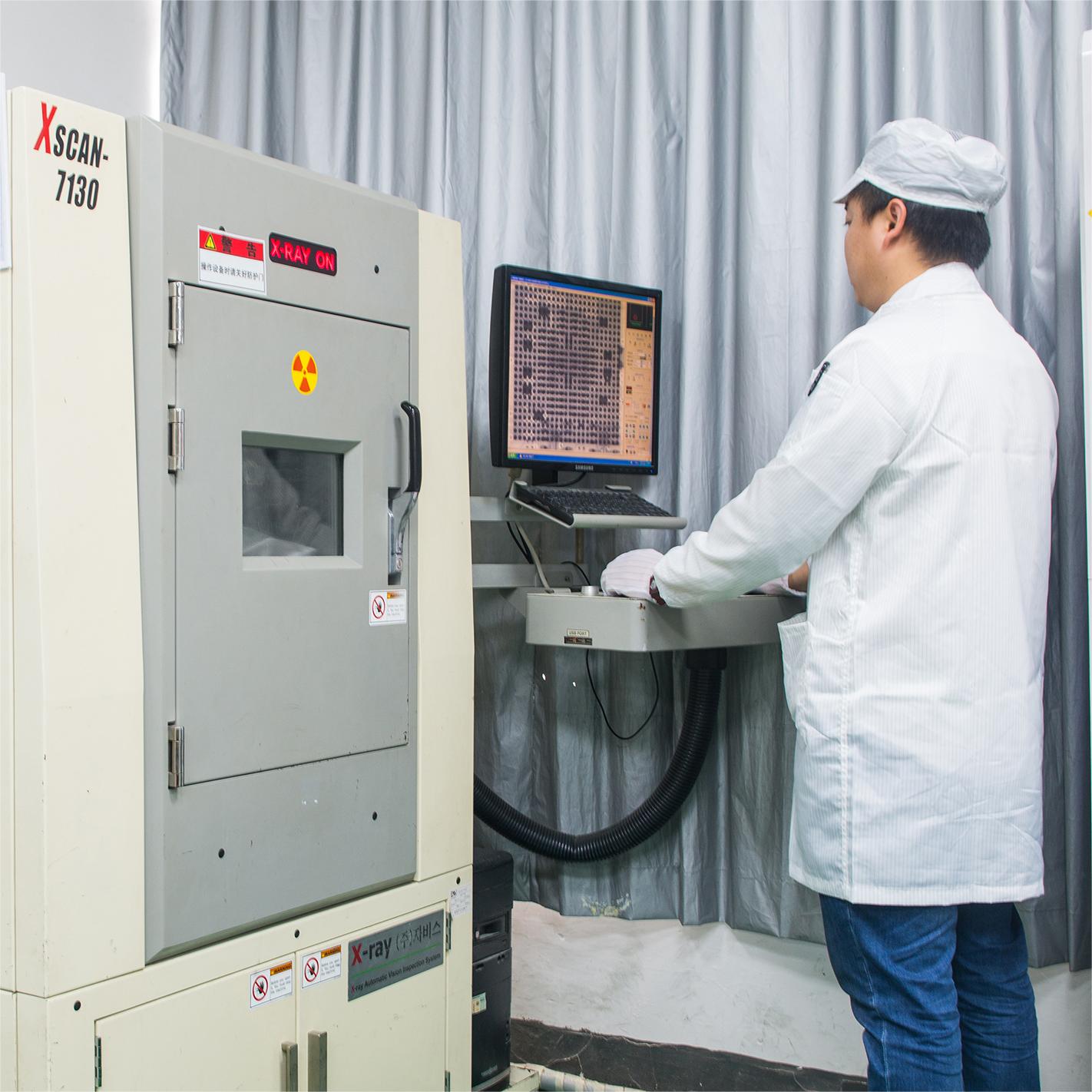
 Quality
 Drills & Throughplating
 Factory & Certificate


-

-
-
-
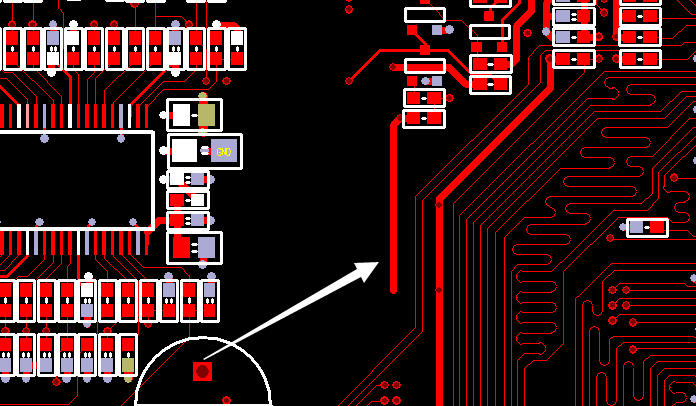
Introduction to Via in Pad Technology
Introducing pcb pad holes and designing it precautions
4409 1 0 Shares
-
-
-
-
-
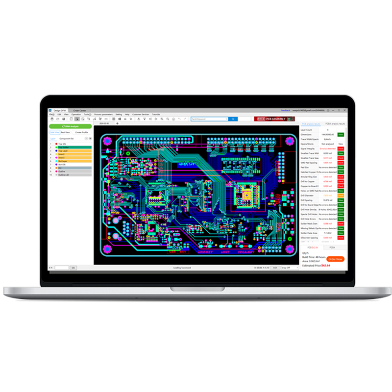
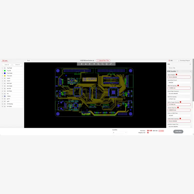
DFM, DFMA, DFA. Part 2. NextPCB's PC program
Detailed example of using the desktop version of HQDFM.
4877 2 0 Shares
-
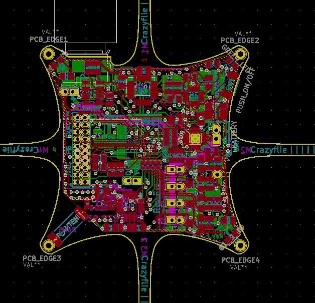
DFM, DFMA, DFA. Part 1. Kicad and Online Gerber Viewer
The comparison of KiCad Gerber Viewer and HQ PCB DFM Gerber Viewer.
6343 4 0 Shares
-
Как экспортировать файлы Gerber из Altium PCB
How to export Gerber files from Altium PCB in Russian
3037 0 0 Shares
-
-
-
-
-
-
-
-
-

Categories
Recommended Article:
- Selecting an ISO 13485 PCB Assembly Partner for Medical Devices
- How to Select an Advanced Automotive-Grade PCB Manufacturer
- OpenClaw Neural-Hardware Accelerator Program
- Rescuing HDI Yield: Pulse Plating & Pre-treatment for Microvia Reliability
- PCB Design for IoT Devices: Layout, Stackup, Power & Reliability Challenges
- 10 HDI PCB Manufacturers Delivering High‑Density Interconnect Solutions
- Back-drill vs Blind/Buried Vias: Cost, Signal Integrity, and Manufacturing Scalability
- At What Frequency Node Must We Switch from FR-4 to Rogers?
- Ultimate PCB Assembly Guide: Prototyping to Mass Production | NextPCB
- How to Reduce PCB Assembly Costs Without Sacrificing Quality (2026 DFM Guide)