
 Surface


Stacy Lu

 NextPCB Capabilities
Printed Circuit Boards
NextPCB Capabilities
Printed Circuit Boards
 PCB Assembly
 Layer Buildup
 SMD-Stencils
 PCB Design-Aid & Layout
 Mechanics
 Quality
 Drills & Throughplating
 Factory & Certificate
 PCB Assembly Factory Show
Certificate
PCB Assembly Factory Show
Certificate
Support Team
Feedback:
support@nextpcb.com


High-speed digital design has entered an era where the printed circuit board (PCB) is no longer a passive substrate but a complex, frequency-dependent component of the system architecture. As data rates for serial interfaces like PCIe 6.0, 112G SerDes, and DDR5 continue to push the boundaries of Nyquist frequencies, hardware engineers face a persistent nemesis: the via stub. For years, the industry has debated the most effective way to eliminate these parasitic resonators while maintaining fiscal responsibility and manufacturing yield. The choice typically narrows down to two advanced fabrication techniques: back-drilling and the implementation of blind or buried vias.
The fundamental tension in this decision lies in the trade-off between mechanical simplicity and architectural density. Back-drilling offers a subtractive, cost-effective way to salvage signal integrity on standard multilayer boards, whereas blind and buried vias—often the cornerstone of High-Density Interconnect (HDI) technology—provide an additive, high-precision solution that fundamentally changes how signals traverse the Z-axis. This report provides an exhaustive analysis of these technologies, drawing on deep manufacturing insights and empirical data to help signal integrity (SI) engineers, layout designers, and procurement managers select the optimal via strategy for their specific frequency and volume requirements.
Table of Contents
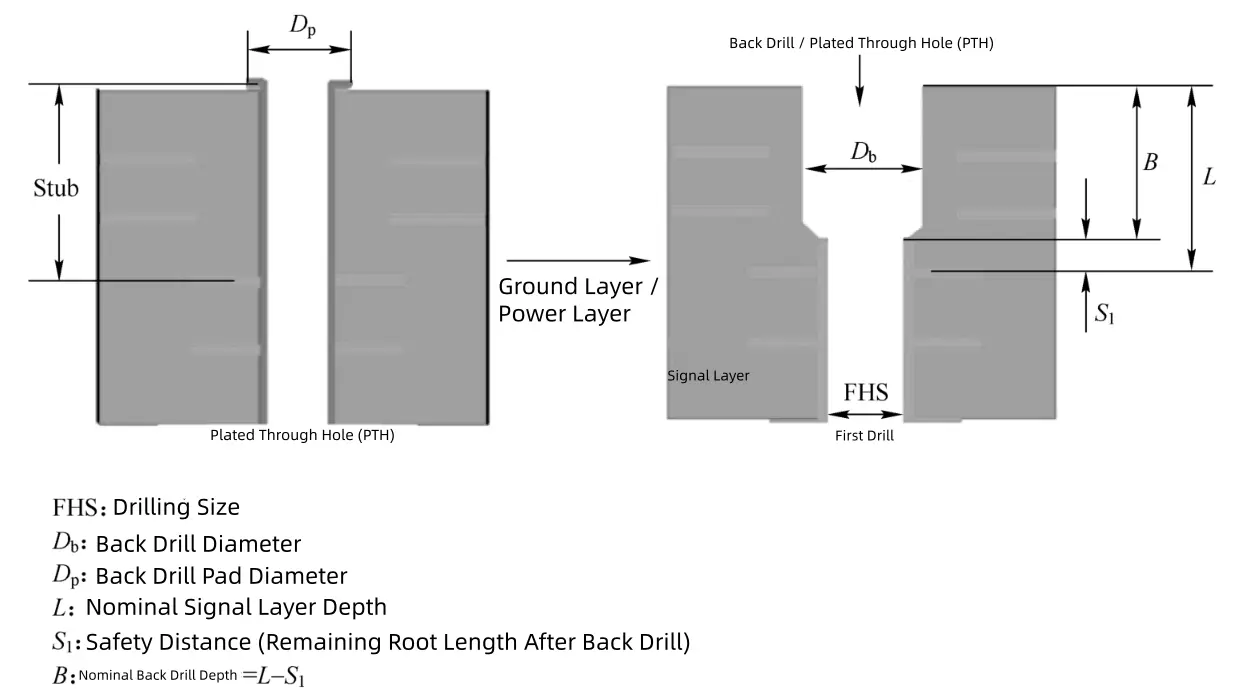
In any multilayer PCB, a plated through-hole (PTH) via is the standard method for transitioning a signal from one copper layer to another. However, the electrical path rarely consumes the entire length of the via barrel. For example, in a 24-layer board, a signal transitioning from Layer 1 to Layer 3 leaves a copper "stub" extending from Layer 4 all the way down to Layer 24. In the DC and low-frequency regime, this stub is negligible. But as frequencies enter the gigahertz range, the stub begins to behave as an unterminated transmission line—a resonator that stores and reflects energy back into the primary signal path.
The primary mechanism of degradation is the quarter-wave resonance. When the electrical length of the stub equals one-fourth of the signal's wavelength, the impedance at the junction where the signal exits the via drops to near zero, causing a massive reflection. This manifest in the frequency domain as a "notch" or a "suck-out" in the insertion loss (S21) plot. If this notch falls near the Nyquist frequency of the data link—for instance, 14 GHz for a 28 Gbps NRZ signal—the resulting inter-symbol interference (ISI) will cause the eye diagram to close, leading to unrecoverable bit errors.
Furthermore, stubs introduce parasitic capacitance. This extra capacitance lowers the characteristic impedance of the via structure, creating a discontinuity. In a 100-ohm differential pair, an unmitigated via might drop to 70 or 80 ohms, causing reflections that contribute to deterministic jitter. Beyond signal loss, these stubs act as unintended antennas, radiating electromagnetic interference (EMI) that can cause a board to fail regulatory compliance tests.
Back-drilling, or controlled-depth drilling (CDD), is a subtractive manufacturing process that removes the unwanted portion of the via barrel after the board has been plated. It is essentially a "clean-up" operation performed late in the fabrication cycle.
It is a process that employs depth-controlled secondary drilling to remove excess stubs from vias or through-holes. This eliminates the parasitic capacitance effect caused by the stubs, ensures impedance consistency between the via/through-hole and the associated trace, thereby reducing signal reflection, improving signal integrity, and enhancing overall signal quality.
Backdrilling is currently the most cost-effective production technology and the most efficient method for boosting channel transmission performance. However, it does lead to a moderate increase in PCB manufacturing costs due to the additional secondary drilling step.
PCB Back Drilling
The process begins with the standard fabrication of a through-hole PCB. Once the barrels are plated with copper and the outer layers are etched, the board is moved to a high-precision CNC drill. Using a drill bit with a diameter slightly larger (typically 4 to 8 mils larger) than the original via, the machine drills from the back side of the board to a specific depth. This drill bit effectively cuts away the copper plating of the stub, leaving an air-filled or resin-filled void.
The precision of this operation is managed through Z-axis depth control. Modern equipment at advanced facilities like NextPCB utilizes contact-sensing technology to calibrate the exact surface height of each panel, ensuring the drill stops within a tight tolerance (often ±2-3 mils) of the target signal layer. The goal is to leave a "residual stub" that is as short as possible—ideally less than 8 mils—without accidentally severing the connection at the signal exit layer.
Back-drilling is highly favored for its simplicity. Because it is a secondary mechanical step, it does not require the complex sequential lamination cycles associated with blind and buried vias. This keeps the manufacturing yield high and the cost relatively low. It is also extremely versatile; any through-via on a board can be back-drilled, regardless of the layer count.
However, back-drilling does not provide a "perfect" zero-length stub. There is always a residual stub due to manufacturing tolerances and the need for a safety margin to avoid over-drilling. Additionally, the larger drill bit creates a larger "keep-out" zone on the layers it passes through, which can restrict routing density on the back-side layers of the board.
| Parameter | High-end Equipment | Frontier Technology |
|---|---|---|
| Back Drill Diameter (Db) | FHS + 0.25mm (0.010in) | FHS + 0.15mm (0.006in) |
| Back Drill Pad Diameter (Dp) | FHS + 0.10mm (0.004in) | FHS + 0.10mm (0.004in) |
| Minimum Back Drill Spacing | 1.00mm (0.039in) | 0.8mm (0.031in) |
| Back Drill Depth Tolerance | 0.15mm (0.006in) | 0.10mm (0.004in) |
| Stub Length (Stub) (S1) | 0.25mm (0.010in) | 0.15mm (0.006in) |
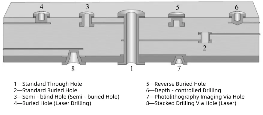
Blind and buried vias represent a fundamentally different philosophy. Instead of removing copper after the fact, these vias are constructed to only span the necessary layers from the very beginning. This is achieved through sequential lamination—a process where sub-sections of the board are built, drilled, and plated before being bonded together.
>> Blind Vias and Buried Vias: What Is the Difference in PCB?
Types of PCB Vias
Blind Vias: These connect an outer layer to one or more internal layers but do not penetrate the entire board. They are "blind" because you can only see them from one side.
Buried Vias: These are entirely internal to the board, connecting two or more inner layers with no connection to the surface. They are "buried" and invisible from the outside.
Microvias: These are a subset of blind/buried vias, typically laser-drilled with a diameter less than 0.15mm (6 mils). They usually span only a single dielectric layer and are the backbone of High-Density Interconnect (HDI) designs.
The primary drawback of blind and buried vias is the manufacturing complexity. Each set of blind or buried vias requires its own drilling, plating, and lamination cycle. For example, a "2+N+2" HDI stackup requires three separate lamination cycles. Each cycle exposes the materials to high temperature and pressure, which can cause material shrinkage, registration errors, and warping. This complexity naturally drives up the cost and lead time of the PCB.
In the pursuit of signal integrity, the choice between back-drilling and blind vias often hinges on the target data rate. The following table compares the typical electrical performance of various via structures based on industry-standard simulations and empirical measurements.
| Feature | Standard Through-Via | Back-Drilled Via | Blind/Buried Microvia |
|---|---|---|---|
| Typical Stub Length | 60 - 250 mils | 4 - 10 mils | < 1 mil |
| Resonant Frequency | 2 - 10 GHz | 30 - 60 GHz | > 100 GHz |
| Impedance Discontinuity | High (15-25%) | Low (5-10%) | Minimal (<5%) |
| Parasitic Capacitance | 0.5 - 1.0 pF | 0.1 - 0.2 pF | < 0.05 pF |
| Crosstalk Coupling | Significant | Reduced | Minimal |
| Ideal Application | Low-speed Digital | 10 - 56 Gbps SerDes | 77 GHz RF / 112G PAM4 |
For signals operating below 5 Gbps, a standard through-via is often acceptable if the stub length is kept reasonably short. As we move into the 10-28 Gbps range (PCIe Gen 4/5, 25G Ethernet), back-drilling becomes the standard "bang-for-the-buck" solution. It pushes the resonance frequency far enough away from the fundamental and third harmonic of the signal to ensure a clean eye diagram.
However, at 56 Gbps and 112 Gbps (PAM4), or for millimeter-wave (mmWave) applications like 77 GHz automotive radar, even a 6-mil residual stub from back-drilling can introduce unacceptable phase noise and insertion loss. In these "ultra-high-speed" scenarios, blind microvias are mandatory. They offer the cleanest possible signal transition with virtually no parasitic load.
Understanding the risks associated with each process is critical for procurement and supply chain managers who must balance performance with reliability.
The risks in back-drilling are primarily mechanical. If the drill depth is too shallow, the stub remains, and the SI issues persist. If the drill is too deep, it can "nick" or completely sever the signal pad on the target layer, resulting in an open circuit or a weak connection that fails during thermal cycling. However, because back-drilling uses larger, mechanically robust drill bits, the plating within the functional part of the via is generally very reliable.
Blind and buried vias face chemical and thermal risks. Plating a deep blind via is difficult because it is hard to get plating chemistry to flow into a "dead-end" hole. This can lead to thin copper at the bottom of the via or "voids" in the plating. Furthermore, because HDI boards undergo multiple lamination cycles, the "Z-axis expansion" of the materials is more pronounced. This puts stress on the via junctions, which can lead to barrel cracking or "lifted pads" during lead-free soldering.
NextPCB mitigates these risks by using state-of-the-art vertical continuous plating (VCP) lines and automated optical inspection (AOI) to ensure uniform copper deposition even in high-aspect-ratio blind vias.
>> NextPCB's Advanced HDI Manufacturing Capabilities
The economic choice between back-drilling and blind vias is heavily influenced by the volume of production and the complexity of the board.
For engineering prototypes and small batches (1-100 units), back-drilling is almost always the winner. It adds roughly 10-20% to the cost of a standard through-hole board because it only requires an extra CNC program and a few minutes of machine time per panel. Creating blind or buried vias for a prototype can double or triple the cost because of the setup required for multiple lamination cycles and the lower initial yields.
In high-volume consumer electronics, the calculation changes. While blind vias are more expensive per square inch, they allow for extreme miniaturization. If using blind vias allows you to shrink a PCB from 6 layers to 4 layers, or reduce the overall board area by 30%, the savings in raw material and enclosure size can offset the higher fabrication cost.
| Metric | Standard PTH | Back-Drilling | Blind/Buried (HDI) |
|---|---|---|---|
| Cost Adder (%) | Base | +10% to +20% | +30% to +100%+ |
| Lead Time Impact | Standard | +1 to 2 Days | +5 to 10 Days |
| Yield Risk | Low | Low-Moderate | Moderate-High |
| Best Volume | Any | Small to Mid | High (Density) |
A via is only as good as the material it passes through. For high-speed designs, the choice of laminate material—specifically its Dielectric Constant (Dk) and Dissipation Factor (Df)—is critical.
NextPCB maintains a robust inventory of these specialty materials, ensuring that high-performance designs don't face supply chain bottlenecks.
>> Rogers vs FR4: How to Choose PCB Materials for High-Frequency Designs
Designing for advanced vias requires a disciplined approach to Design for Manufacturability (DFM). Errors at this stage can lead to unmanufacturable boards or expensive re-spins.
>> Download HQDFM Software for Free Via Stub Analysis
Q1: "I'm routing a 25Gbps Ethernet link on a 16-layer board. My fabricator says back-drilling is much cheaper than blind vias. Is there any catch?"
Answer: The main "catch" is the keep-out zone. Back-drilling requires larger holes on the bottom layers, which might interfere with your routing density there. However, for 25Gbps, back-drilling is the technically sound and fiscally responsible choice. It provides 90% of the SI benefit of blind vias at a fraction of the cost.
Q2: "Can I use back-drilling on a 4-layer board to fix signal issues?"
Answer: Practically speaking, no. On a 4-layer board, the stubs are usually too short to cause significant resonance below 10GHz. Furthermore, most fabricators have a minimum board thickness requirement for back-drilling (usually >0.8mm) to ensure the Z-axis drill can be controlled accurately. If you have SI issues on 4 layers, a stackup change is a better first step.
Q3: "I've heard buried vias are less reliable than through-vias. Should I be worried?"
Answer: Buried vias are very reliable if the manufacturer uses high-quality epoxy fill and proper planarization. The risk only increases if you stack multiple microvias on top of each other. For the highest reliability, use "staggered" microvias instead of "stacked" ones, as this distributes mechanical stress more evenly.
Q4: "My EDA tool shows the back-drill as a 'hole' in the 3D view. Does this mean I lose routing space on those layers?"
Answer: Yes. That is the one major trade-off of back-drilling. The back-drill bit removes copper on all layers from the entrance side down to the target layer. You cannot route any signals through that "hole" on those layers. Blind vias, conversely, leave those layers completely open for routing.
Q5: "How do I specify back-drilling in my Gerber files? Is a separate drill file enough?"
Answer: A separate drill file is a good start, but you must also include a "Back-Drill Schedule" or "Fabrication Note" in your readme file. Explicitly state the via nets, the start layer, the stop layer, and the required residual stub length. Advanced tools like the HQDFM viewer can help you verify these settings before ordering.
Selecting between back-drilling and blind/buried vias is not just a technical decision; it is a strategic one that impacts your product's time-to-market and bottom line.
When to use Back-Drilling:
When to use Blind and Buried Vias:
NextPCB is uniquely positioned to support engineers through this entire journey. From our free HQDFM analysis that catches via errors before they happen, to our world-class fabrication facilities capable of 32+ layers and HDI III structures, we ensure your high-speed design performs exactly as simulated.
Ready to optimize your next high-speed project?
Don't leave your signal integrity to chance. Upload your Gerber files to (https://www.nextpcb.com/) for an instant quote and a comprehensive DFM review. Our technical team is standing by to help you refine your stackup and via strategy for maximum performance and cost-efficiency.

Still, need help? Contact Us: support@nextpcb.com
Need a PCB or PCBA quote? Quote now

