

 NextPCB Capabilities
 PCB Assembly
 Layer Buildup
 SMD-Stencils
 PCB Design-Aid & Layout
 Mechanics
 Surface
 Quality
 Drills & Throughplating
 Factory & Certificate


Here are some important considerations for silk screen design in PCB manufacturing:
1、Silk Screen Character Design:
- The ratio of word height to word width should be ≥ 6:1 to ensure legibility.
- For high-density boards, 4/25mil characters are commonly used.
- For normal density boards, it is recommended to use 5/30mil characters.
- For loose boards, 6/45mil characters are recommended.
2、Silk Screen Width Requirements:
- The wire width of silk screen should be greater than or equal to 4mil.
- The thickness of the surface base copper affects silk screen width:
- For copper base thickness <1OZ, the limit value should be ≥ 4mil, and the optimization value should be ≥ 6mil.
- When the thickness of base copper is 1oz, it is preferable to use 5/30mil characters for silk screen printing.
- When the thickness of base copper is 2OZ, it is preferable to use 6/45mil characters for silk screen printing.
3、Silk Screen Spacing Requirements:
- Maintain a minimum spacing of 6mil between silk screen printing and silk screen printing to avoid overlap and ensure clarity.
- Maintain a minimum spacing of 6mil between silk screen printing and pad to prevent interference and readability issues.
4、Silk Screen Placement - Required:
- The reading direction of silk screen printing should align with the use direction of the board to facilitate assembly and maintenance processes, minimizing the chances of reverse welding.
- Follow the principle that the string is from left to right or from bottom to top for consistent and readable silk screen layout.
- For special packages like BGA and QFN, the size of silk screen printing should precisely match the size of the chip to aid in accurate component placement.
- Add screw silk screen near installation holes, marking the length and total number of screws, for easy and efficient installation.
5、Silk Screen Placement - Avoid:
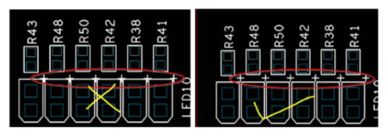
- Avoid covering welding points, test points, and mark points with silk screen printing, as it may hinder inspections and lead to errors during assembly.
- Do not place silk screen on high-speed signal lines, such as clock lines, to prevent signal integrity issues.
6、Device Location:
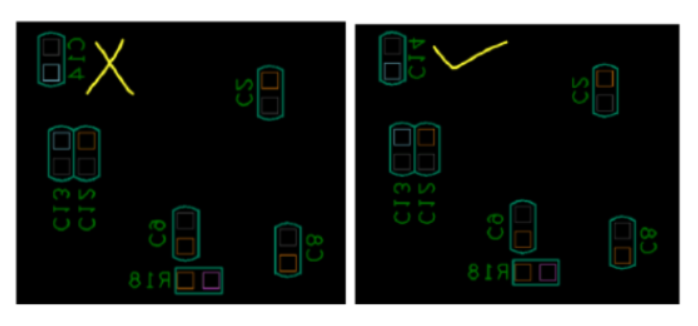
- Ensure that the silk screen corresponds to each device accurately, without any reversals or changes in sequence.
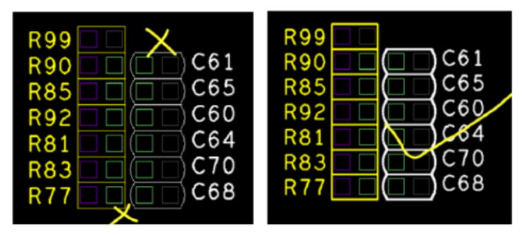
- For densely populated boards, consider leading-out labeling or symbol labeling to accommodate additional information. Place these elements on the silk screen layer of the board geometry.
- If there is limited space for the seat number, provide assembly drawings to facilitate device installation and inspection.
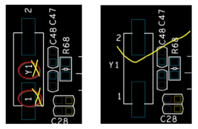
- Never place the device bit number inside the device or outside the plate frame; it should be clearly visible and appropriately positioned.
- Polarity marks and "1" foot marks of components should be placed correctly and clearly to avoid any assembly mistakes.
Examples of FAQs and Solutions:
1、Welding Resistance on Characters, Incorrect Device Bit Number: If welding resistance occurs on characters or the device bit number is not adjusted correctly, review the silk screen design files, and ensure the characters are adequately spaced from pads and components. Verify that the device bit numbers are correctly aligned with the devices on the PCB.
2、Thin Line Width of Characters and Silk Screen Printing: If the line width of characters and silk screen printing is too thin, adjust the line thickness in the silk screen design software to meet the minimum width requirements and improve legibility.
3、Inconsistent Character Directions: Inconsistent character directions can lead to confusion during assembly and maintenance. Make sure all characters have a uniform orientation, either horizontally or vertically, as per the reading direction.
4、Unclear Polarity Identification: Unclear polarity identification can cause serious issues during PCB assembly and circuit operation. Double-check and ensure the polarity marks are correctly placed and clearly visible for all components.
By following these precautions and addressing common issues, you can create an effective and error-free silk screen design for your PCBs, leading to smoother manufacturing and better product quality. For professional PCB manufacturing services, check out NextPCB for top-notch solutions.

