
 NextPCB Capabilities
Printed Circuit Boards
NextPCB Capabilities
Printed Circuit Boards
 PCB Assembly
 Layer Buildup
 SMD-Stencils
 PCB Design-Aid & Layout
 Mechanics
 Quality
 Drills & Throughplating
 Factory & Certificate
 PCB Assembly Factory Show
Certificate
PCB Assembly Factory Show
Certificate
Support Team
Feedback:
support@nextpcb.com


The Printed Circuit Board (PCB) is the backbone of modern electronic devices, providing the necessary connections between various components. One critical aspect of PCB design is the strategic placement and implementation of vias, especially within the pads. This article delves into the significance of vias in pads, their role in PCB functionality, and the technical considerations involved in their design and use.
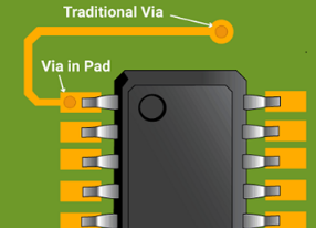
Vias are small holes that pass through the layers of a PCB to create electrical connections between different layers. A pad, on the other hand, is a rectangular or square area on the PCB used to mount components or make connections. When a via is placed within a pad, it is referred to as a "via in pad." This design allows for the vertical interconnection of conductive paths, which is crucial for complex multi-layer PCBs.
Vias in pads serve several essential functions within the PCB design:
1, Interlayer Connection: The primary role of a via in a pad is to connect different layers of the PCB, enabling the flow of electrical signals or power supply between them.
2, Component Mounting: In some cases, a via in a pad can be used as a mounting point for components. This is particularly useful when the component lead or pin is designed to pass through the pad and be soldered directly to the via.
3, Signal Integrity: Strategically placed vias in pads can help maintain signal integrity by providing the shortest possible path for signals to travel between layers, reducing cross-talk and signal degradation.
4, Thermal Management: Vias can also aid in the dissipation of heat within the PCB. They can be used as thermal vias, which help to draw heat away from critical components and distribute it across the board.
Designing vias within pads involves several technical considerations to ensure optimal performance and reliability:
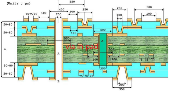
1, Size and Spacing: The size of the via should be appropriate for the size of the pad and the current it is expected to carry. The spacing between vias within a pad or between adjacent pads must also be considered to prevent short circuits and ensure sufficient heat dissipation.
2, Material Compatibility: The materials used for the PCB layers, pads, and vias must be compatible to ensure reliable electrical connections and long-term durability.
3, Drilling Precision: The drilling process for creating vias must be precise to avoid damaging the PCB layers or affecting the alignment of components.
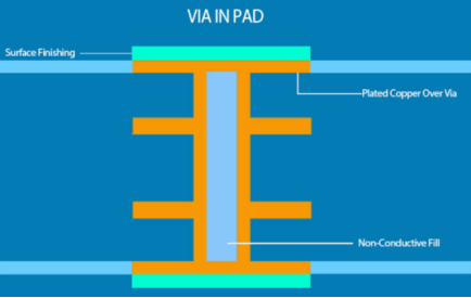
4, Soldering and Plating: The vias in pads must be properly plated to ensure a reliable electrical connection and to prevent oxidation. The soldering process must also be controlled to ensure a strong bond between the via, pad, and component lead.
Vias in pads are a fundamental aspect of PCB design, enabling the complex interconnections required for today's sophisticated electronic devices. They play a critical role in the performance, reliability, and thermal management of PCBs. By understanding the technical considerations and best practices in designing and implementing vias in pads, engineers and designers can create PCBs that meet the demands of modern electronic applications. As technology continues to advance, the importance of precision and innovation in PCB design, including the strategic use of vias in pads, will only continue to grow.
Still, need help? Contact Us: support@nextpcb.com
Need a PCB or PCBA quote? Quote now


 Surface

