
 Surface


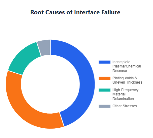
- Distribution of physical root causes leading to microvia fracture under thermal cycling.
- Incomplete desmear and uneven plating form the bulk of structural weaknesses.

 NextPCB Capabilities
Printed Circuit Boards
NextPCB Capabilities
Printed Circuit Boards
 PCB Assembly
 Layer Buildup
 SMD-Stencils
 PCB Design-Aid & Layout
 Mechanics
 Quality
 Drills & Throughplating
 Factory & Certificate
 PCB Assembly Factory Show
Certificate
PCB Assembly Factory Show
Certificate
Support Team
Feedback:
support@nextpcb.com


Core Summary: Microvia fracture in High Density Interconnect (HDI) boards is one of the main causes of product failure in thermal cycling tests. In engineering practice, the failure of the bonding force at the bottom of the microvia is a common focus. Combined with 15 years of EMS experience, this article deeply analyzes how to solve the bonding force and plating uniformity issues at the Target Pad interface through plasma and chemical dual Desmear, lamination parameter optimization, and Periodic Pulse Reverse (PPR) plating technologies, ensuring the product meets the IPC-6012E reliability standard.
In hardware engineering and PCB procurement, the microvia reliability of HDI boards has always been a core challenge. In engineering practice, when the microvia diameter is close to 0.1 mm, yield and reliability are often more susceptible to process fluctuations.
In routine bare board electrical testing, the conductivity of blind vias often appears normal; however, when subjected to the high-temperature shock of PCBA secondary lead-free reflow soldering (usually close to 260℃), the copper layer at the bottom of the microvia is often torn apart due to severe Z-axis Coefficient of Thermal Expansion (CTE) stress. This target pad failure phenomenon is highly concealed and is the main cause of high-value PCBA scrapping.
Table of Contents
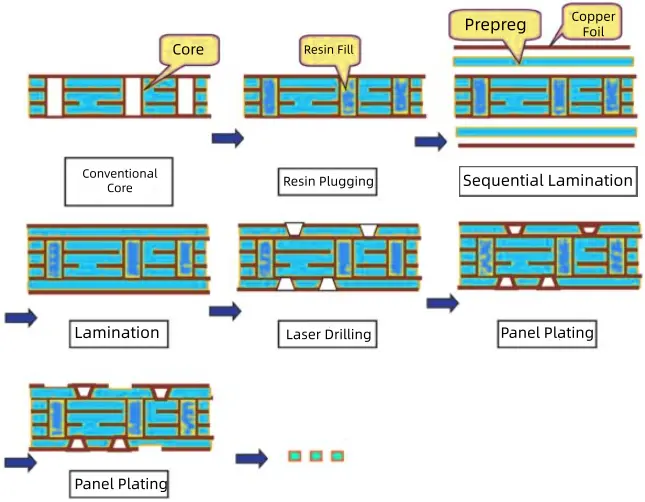
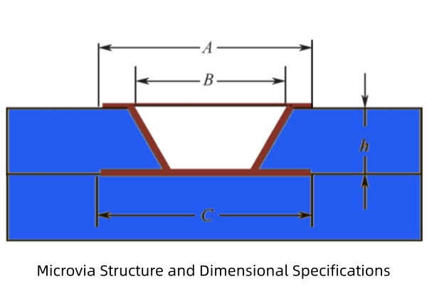
HDI microvia manufacturing process including laser drilling, desmear treatment, pulse plating, and sequential lamination to enhance microvia reliability
Microvia failure mainly occurs at the bonding interface between the electroplated copper at the bottom of the hole and the Target Pad. In addition to common physical stress, the following two factors are the culprits causing a fragile interface:
Under the pulling of the Z-axis thermal expansion stress brought by lead-free soldering (caused by the mismatch of the CTE thermal expansion coefficient between the PCB dielectric layer and copper), the interface with the weak physical bonding strength mentioned above is prone to mechanical separation.
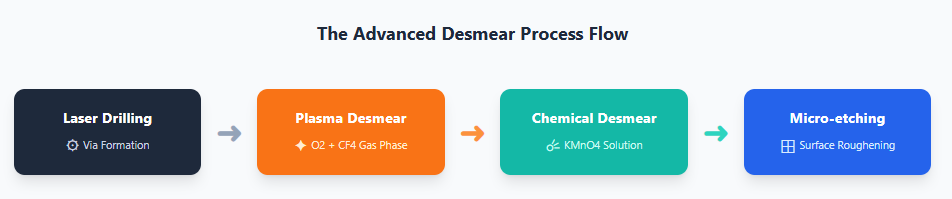
High-quality electroplating results highly depend on the pre-treatment process after drilling. The traditional single chemical potassium permanganate desmear solution, when dealing with the micro-hole diameters of high-order HDI (such as 2-N-2 or Any-layer), is limited by the surface tension of the liquid and is difficult to fully penetrate to the bottom of the hole.
In community discussions, many engineers mentioned the "delamination nightmare" of high-frequency materials. When using Low Loss materials with poor resin fluidity, if the process control is improper, it is extremely easy to cause Measling or Crazing in dense via areas.
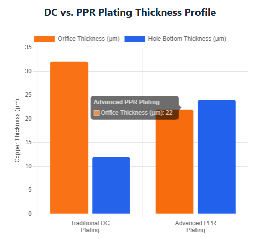
Traditional Direct Current (DC) plating has obvious process limitations in microvia filling, which is prone to causing early closure of the orifice, thereby triggering internal voids. To ensure the specified copper thickness is reached at the bottom of the hole, the surface of the orifice is often over-deposited. This not only increases the difficulty of subsequent outer layer circuit etching (especially high-precision L/S) but may also lead to early closure of the orifice and the formation of internal voids. Pulse Periodic Reverse (PPR) plating is an effective solution to overcome this bottleneck.
PPR does not use constant direct current, but alternately applies forward and reverse pulses within a millisecond-level cycle.
Process effectiveness: PPR achieves a standard "Bottom-up Filling". A dense, crystal-defect-free pure copper structure can be formed inside the microvia, while the surface copper thickness is precisely controlled. In microsection analysis, blind vias plated with PPR show a dense filling structure (usually an inverted cone/inverted trapezoid shape), which can significantly enhance its ability to resist thermal stress and help the product meet the thermal shock test requirements specified in IPC-6012E.
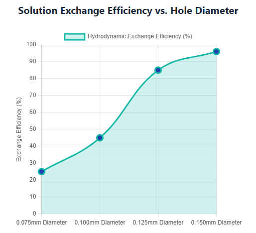
Exponential increase in chemical exchange efficiency observed when shifting diameter from 0.100mm to 0.125mm, drastically reducing the risk of internal voiding.
Although the design end tends to pursue extremely small hole diameters to save routing space, practical experience shows: excessively pursuing reduced hole diameters is often at the expense of yield.
When evaluating HDI suppliers, it is recommended to pay attention to the following engineering details to avoid potential risks:
Q1: Why do my microvias pass flying probe tests but fail after SMT?
A: This is typically due to latent defects at the Target Pad interface. Flying probe tests are conducted at room temperature with minimal mechanical stress. During SMT reflow, temperatures reach 260℃, causing the PCB material to expand significantly in the Z-axis. If the bonding between the plated copper and the target pad is weak (due to poor desmear or DC plating issues), the CTE mismatch stress will pull the interface apart, creating an open circuit that only manifests after thermal exposure.
Q2: Is Plasma Desmear mandatory for all HDI boards?
A: While not strictly mandatory for simple HDI, it is highly recommended for any design with microvias ≤ 0.1mm or those using high-performance/low-loss resins. Chemical desmear relies on liquid penetration, which is hindered by air bubbles and surface tension in tiny holes. Plasma is a gas-phase process that ensures 100% removal of resin smear at the hole bottom, providing a reliable foundation for copper bonding.
Q3: How does PPR plating prevent "Dog-boning"?
A: "Dog-boning" (thick copper at the orifice and thin copper in the hole) occurs in DC plating because current concentrates at the corners. PPR uses reverse pulses to strip away excess copper from high-current-density areas (the orifice) while deposition continues at the bottom. This dynamic balancing ensures a flat surface and a fully filled hole, which is critical for stacked via reliability.
Q4: What is the ideal aspect ratio for microvias to ensure high yield?
A: For optimal reliability and plating quality, an aspect ratio of 0.75:1 or less is ideal. For example, if your dielectric thickness is 75 microns, a hole diameter of 100 microns (0.1mm) is recommended. Pushing the aspect ratio beyond 1:1 significantly increases the risk of voids and thin hole-wall plating.
The physical reliability of microvias is directly related to the life cycle of the terminal product. NextPCB.com focuses on high-precision PCB manufacturing, equipped with high-end automated electroplating production lines and precision laser drilling technology to ensure the quality and stability of microvias in complex interconnects. We not only provide manufacturing services but also deeply participate in design reviews relying on senior engineering teams and HQDFM digital tools, assisting engineers in reaching the best fit between "design density" and "manufacturing yield".
>> To learn more about high-reliability HDI solutions, welcome to visit NextPCB for professional technical support.
>> Visit All Advanced PCB Manufacturing Capabilities at NextPCB
Still, need help? Contact Us: support@nextpcb.com
Need a PCB or PCBA quote? Quote now

