
 NextPCB Capabilities
Printed Circuit Boards
NextPCB Capabilities
Printed Circuit Boards
 PCB Assembly
 Layer Buildup
 SMD-Stencils
 PCB Design-Aid & Layout
 Mechanics
 Quality
 Drills & Throughplating
 Factory & Certificate
 PCB Assembly Factory Show
Certificate
PCB Assembly Factory Show
Certificate
Support Team
Feedback:
support@nextpcb.com


Introduction
The rapid growth of Internet of Things (IoT) devices has reshaped how electronic hardware is designed. Unlike traditional products, IoT devices must be compact, energy-efficient, continuously connected and reliable over long periods—often operating in harsh or unattended environments. As board sizes shrink and functionality increases, PCB design becomes a critical factor in product performance, not just a supporting step in development.
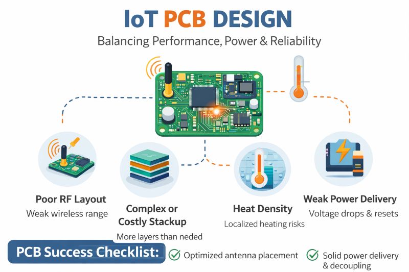
Key challenges in IoT PCB design including RF layout discipline, stackup planning, heat density, and stable power delivery
In many IoT projects, failures stem from PCB-level issues such as unstable power delivery, poor signal integrity, RF layout mistakes, or environmental stress—not from firmware or cloud systems. Designers must balance limited board space, low-power operation, mixed-signal integration and wireless reliability within strict cost and manufacturing constraints. This article explores the practical PCB design strategies that help engineers build stable, scalable, and production-ready IoT devices.
IoT PCBs rarely fail because of one big mistake. They fail because multiple design pressures collide on a very small board. Before layout begins, it’s important to understand what is actually pushing the design.
Compact enclosures reduce board area. Components sit closer together, routing channels shrink, and grounding becomes harder.
PCB impact: Multilayer layouts — and sometimes HDI — are required just to route cleanly.
Wireless transmission creates short but high current spikes.
PCB impact: Short power paths, solid ground reference, and proper decoupling are essential to prevent resets and noise.
Wireless modules require controlled impedance and isolation from digital switching noise.
PCB impact: Proper antenna placement, continuous ground planes, and strict RF zoning are mandatory.
IoT devices face temperature cycling, humidity, and vibration.
PCB impact: Stackup symmetry, material selection, and environmental protection directly affect lifespan.
Large-scale IoT deployment demands cost efficiency.
PCB impact: Use the simplest stackup that meets requirements - avoid unnecessary layers or HDI features.
PCB layout is one of the most critical—and most challenging—stages in IoT hardware development. Poor layout decisions at this stage often lead to signal noise, wireless performance issues, excessive power drain, or costly redesigns.
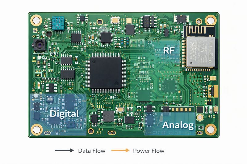
Separating digital, RF, and analog zones improves signal integrity and reduces interference in compact IoT boards
| Challenge Area | What Creates the Problem | What Goes Wrong | Practical Design Focus |
|---|---|---|---|
| High Component Density | Small board size with MCU, RF, sensors, power on one PCB | Routing congestion, EMI, crosstalk, difficult fanout | Use multilayer stackup, optimize placement first, shorten critical paths |
| Limited Routing Space | Fine-pitch components and tight spacing | Long traces, extra vias, layer count increase | Plan escape routing early, minimize via transitions |
| Mixed-Signal Interference | Digital, analog, RF and power circuits on same board | Noise coupling into sensors, unstable wireless | Separate functional zones, maintain solid ground planes |
| Grounding & Return Path Issues | Split planes, poor zoning, uncontrolled routing | Crosstalk, EMI, unstable measurements | Keep ground continuous, control return paths |
| RF Layout Constraints | Antenna placement limits, small enclosure | Reduced range, unstable connectivity | Place antenna at board edge, define keep-out zones |
| Impedance Control | RF traces without controlled stackup | Signal reflections, poor transmission efficiency | Use defined stackup and controlled impedance routing |
| RF & Digital Coupling | Clocks and switching regulators near RF path | Communication dropouts, higher power consumption | Isolate RF section from noisy digital circuits |
Stackup selection is one of the earliest—and most expensive to change—decisions in IoT PCB design. The right stackup simplifies routing, improves signal integrity, and controls cost. The wrong one leads to noise issues, rework, or unnecessary manufacturing complexity.
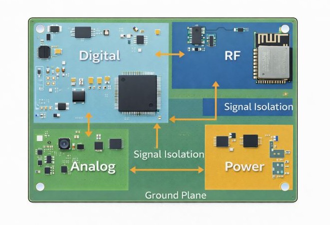
Signal isolation and a solid ground plane are essential for stable RF and mixed-signal IoT designs
For most IoT devices, simpler stackups deliver better cost and reliability when chosen correctly.
Choose a 2-layer PCB if:
Typical use: Basic sensors, simple control boards
Choose a 4-layer PCB if:
As integration increases, routing density and signal quality drive stackup decisions.
Move to 6 layers or more when:
Warning: More layers increase cost and lead time—optimize routing first before adding layers.
HDI stackups should be used only when traditional multilayer designs fail.
HDI is justified if:
Practical guidance:
Before routing begins, confirm:
Early stackup alignment reduces rework and improves first-pass success.
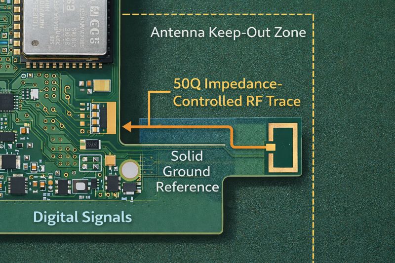
Correct antenna placement with 50Ω controlled impedance routing improves wireless range and stability
IoT devices operate in short active bursts followed by long sleep periods, creating a mismatch between average and peak current demand. During wireless transmission, sudden current spikes can cause voltage droop, random resets, noisy sensor readings, or unexpected battery drain. These issues are typically not schematic errors—they are layout problems caused by long power traces, poor decoupling placement, and weak ground return paths.
Strong power integrity starts with placement. Regulators should sit close to their loads, supply paths should be short and wide (or use power planes), and decoupling capacitors must be placed directly at IC power pins. Even small layout changes—such as moving a capacitor closer to the MCU—can eliminate stability issues during RF bursts.
Thermal behavior also matters in compact boards. Concentrated heat around regulators, MCUs, or radios can reduce reliability over time. Proper copper distribution, thermal vias, and component spacing help maintain long-term stability.
If firmware timing changes affect hardware stability, the root cause is usually PCB power layout—not software. In compact IoT designs, reliable operation begins with disciplined power distribution and grounding.
In real IoT deployments, most failures do not happen in the lab—they happen months later, in the field. Devices that pass functional testing can still fail due to environmental exposure, aging, or subtle PCB design weaknesses. Reliability in IoT is therefore less about specifications and more about how a PCB behaves over time under real operating conditions.
Based on common deployment scenarios, the most frequent PCB-level failures include:
These failures are often gradual and difficult to reproduce in development environments.
IoT devices are routinely exposed to conditions far more severe than office electronics.
Real-world stress factors:
What works in practice:
In IoT projects, many hardware issues arise not from circuit design, but from gaps between design intent and manufacturing reality. Because IoT devices are often produced in high volumes and deployed long-term, early attention to manufacturability and process consistency is essential for controlling cost, yield, and reliability.
Design-for-Manufacturability (DFM) ensures that a PCB layout can be fabricated and assembled consistently using standard production processes. In IoT designs—where boards are compact and densely populated—DFM considerations should be addressed from the earliest layout stage.
Key DFM factors include:
Ignoring DFM until late in the project often leads to layout revisions, delayed schedules, and increased production cost.
IoT devices are typically cost-sensitive, especially in large-scale deployments. PCB cost is influenced by layer count, material selection, via structures, and manufacturing complexity.
Practical cost-control strategies include:
Evaluating cost at the system level is important—slightly higher PCB cost can often reduce assembly complexity or improve field reliability.
Manufacturing timelines are a critical factor in IoT product development. Lead times can be affected by PCB complexity, material availability, and component sourcing.
To minimize delays:
Early coordination between design, sourcing, and manufacturing teams helps ensure predictable delivery schedules.
HDI PCBs are a powerful solution for compact and high-performance IoT devices, but they are not required for every design. Knowing when HDI adds real value—and when it does not—is essential for balancing performance, cost, and manufacturability.
HDI PCBs become a practical choice when traditional multilayer designs can no longer meet layout or performance requirements. Common indicators include:
For simple IoT products with low-speed signals and minimal space constraints, a conventional 4-layer PCB may be sufficient. However, as device complexity increases, traditional designs often lead to larger boards, longer signal paths, or compromised performance.
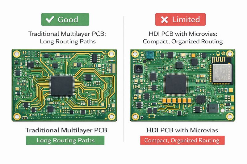
HDI PCBs enable compact routing and improved signal integrity compared to traditional multilayer designs
HDI PCBs offer:
The decision should be based on actual design constraints, not on adopting HDI by default.
HDI PCBs are commonly used in IoT devices such as:
In these applications, HDI enables smaller form factors, stable wireless performance, and reliable operation over long deployment periods.
Many IoT PCB issues arise from avoidable design decisions that only surface late in development or after field deployment. Identifying these mistakes early helps reduce redesigns, control cost, and improve first-pass manufacturing success.
Poor Antenna and RF Placement: Improper antenna placement often causes weak or unstable wireless performance. Placing the antenna too close to ground, metal, batteries, or noisy signals reduces range and increases power use. Always respect antenna keep-out zones and consider enclosure effects during layout.
Overlooking Power Integrity: Power integrity is often underestimated. Long or thin power traces, poor decoupling placement, and weak grounding can lead to voltage drops, random resets, sensor noise, and reduced battery life. Power delivery must be optimized during PCB layout—not just at the schematic stage.
Over-Engineering the Stackup: Using unnecessary layers, stacked microvias, or advanced materials without clear need increases cost and lead time. Stackup complexity should be driven by routing and performance requirements, not assumptions.
Delaying DFM Review: Skipping early DFM checks can lead to fabrication issues such as unsupported vias, tight tolerances, and assembly challenges. Early collaboration with manufacturers like NextPCB helps validate designs and avoid costly late-stage changes.
IoT PCB design is shifting from basic connectivity toward high integration, long-term reliability, and scalable manufacturing. As devices become smaller and more capable, PCB decisions will increasingly determine product lifespan, power efficiency, and deployment success.
| Area | 2026 Reality | 2030 Direction |
|---|---|---|
| Integration | Multilayer & selective HDI | Widespread HDI & advanced packaging |
| Wireless | Single or dual protocols | Multi-protocol coexistence standard |
| Power | Battery-focused layouts | PCB-level energy optimization |
| Manufacturing | DFM encouraged | DFM mandatory for scale |
| Sustainability | Compliance-driven | Design-driven responsibility |
Here are some common FAQs related to PCB Design for IoT Devices:
The best PCB depends on complexity. Simple IoT devices use 2- or 4-layer boards, while compact or high-performance designs often require multilayer or HDI PCBs.
No. HDI PCBs are needed only when board size is limited, component density is high, or fine-pitch BGAs and RF routing cannot be handled by standard PCBs.
Most IoT devices work well with 4-layer PCBs. More complex designs with dense routing or RF requirements may need 6 layers or HDI structures.
Good PCB design reduces power loss by shortening power paths, placing decoupling capacitors correctly, minimizing noise, and improving power integrity, which extends battery life.
Major risks include moisture, temperature cycling, poor RF layout, unstable power delivery, and manufacturing issues. These can be reduced with proper materials, layout, and early DFM review.
RF layout is critical. Antenna placement, grounding, impedance control, and isolation from digital noise directly affect wireless range, stability, and power efficiency.
Yes. IoT PCBs can be produced in low volumes for prototypes or pilot runs, especially when early coordination with the manufacturer ensures feasibility and cost control.
In conclusion, we say that designing PCBs for IoT devices requires balancing size, power efficiency, signal integrity, reliability, and manufacturability. As IoT hardware becomes more compact and complex, early decisions around layout, stackup, power delivery, RF design, and DFM planning have a direct impact on cost, performance, and long-term reliability. With increasing demands from wireless connectivity and real-world deployment conditions, aligning PCB design with manufacturing capabilities is critical. From a manufacturing perspective, NextPCB supports this process by combining advanced PCB technologies with practical engineering guidance to help OEMs bring scalable and reliable IoT products to market.
Still, need help? Contact Us: support@nextpcb.com
Need a PCB or PCBA quote? Quote now


 Surface

