
 Surface


Arya Li, Project Manager at NextPCB.com

 NextPCB Capabilities
Printed Circuit Boards
NextPCB Capabilities
Printed Circuit Boards
 PCB Assembly
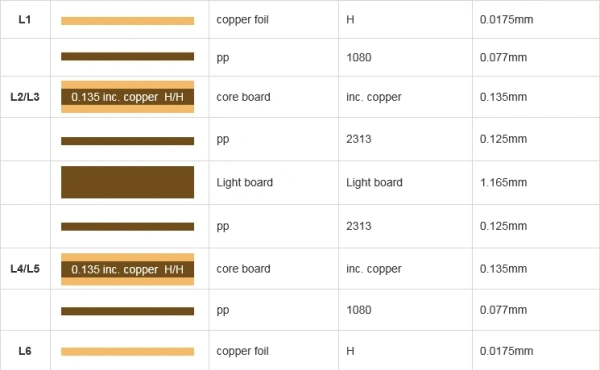
 Layer Buildup
 SMD-Stencils
 PCB Design-Aid & Layout
 Mechanics
 Quality
 Drills & Throughplating
 Factory & Certificate
 PCB Assembly Factory Show
Certificate
PCB Assembly Factory Show
Certificate
Support Team
Feedback:
support@nextpcb.com


Introduction
Printed circuit boards, sometimes known as PCBs, define the heart of today's electronics. For most gadgets, they form the primary structural component. A fundamental component of PCB design is layer stack-up. This relates to the configuration of copper and insulating layers making up the PCB. This arrangement influences several important factors from cost to manufacturing simplicity to electrical capacity. This paper seeks to address PCB layer stack-up. It will discuss its relevance, several configurations, and advice on building an efficient stack-up.
Contents
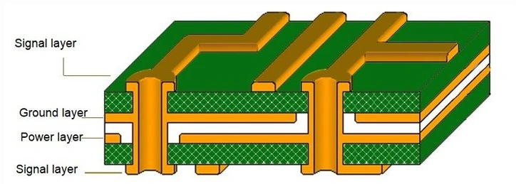
The signal, power, and ground layers set inside a PCB determine whether specific design criteria apply. Reaching the ideal mechanical and electrical performance requires this specific configuration. Good design of a stack-up can increase general product dependability, lower electromagnetic interference (EMI), and enhance signal integrity (SI). Usually found alternately on a PCB, conductive copper, and insulating material are the layout and operation of these layers define the overall PCB performance. For example, whereas signal layers transmit electrical signals, power, and ground planes provide constant references for power distribution. Made of FR-4 or another material, insulating layers help to separate the conducting layers and prevent any possible electrical short connections.
> Recommend reading: Best 6-Layer PCB Stackups for Signal Integrity & Impedance Control
The stack-up design of a PCB is crucial for various aspects of the board's functionality, such as:
1. Electromagnetic Compatibility (EMC): Reducing both differential-mode and common-mode emissions using the suitable layer stack-up is essential to follow EMC rules. EMC-abiding electronic equipment will not interact with other devices and will run regularly within its intended surroundings.
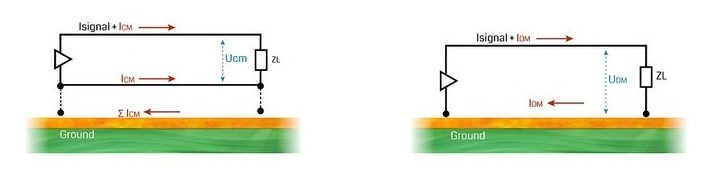
2. Signal Integrity (SI): A good stack-up ensures that signal traces have a constant impedance, therefore reducing signal reflection and crosstalk. For circuits at high speeds in both digital and RF domains, signal integrity is critical since even the smallest drop in signal quality may cause data errors or device malfunction.
3. Power Integrity (PI): Stack-up can reduce voltage changes and make sure that every part gets a steady source of power by carefully placing the power and ground planes. This is very important for complicated circuits that need a lot of energy and more than one power domain.
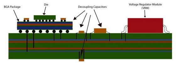
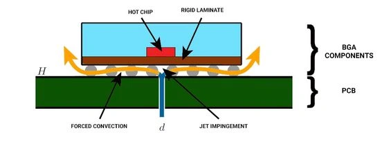
4. Thermal Management: Effective layer organization is essential for maximizing heat dissipation in high-power applications. Proper temperature management of electronic components increases their longevity. Overheating can lead to breakdowns.
A printed circuit board (PCB) can be classified according to its layer count:
Multilayer printed circuit boards (PCRs) are advised to be used for frequencies above 10 MHz since they emit far less radiation than 2-layer boards. These qualities make them suitable for use in several contexts, including computers, cell phones, and high-frequency communication tools.
A typical 4-layer PCB stack-up might include:
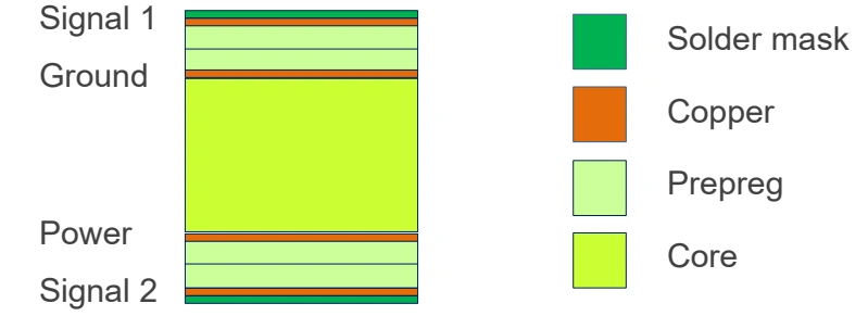
This configuration offers three primary advantages. One advantage is a reduction of approximately 10dB in trace loop radiation because of the tight coupling between the signal and reference plane. Furthermore, reducing the plane impedance decreases the emission of common mode radiation originating from wires connected to the board. In conclusion, the substantial decrease in interference between electrical traces results in an improvement in the overall quality of the signal.
This setup saves cash, but its protection and electromagnetic interference (EMI) restrictions are a problem. A different 4-layer stack organization possibility could be:
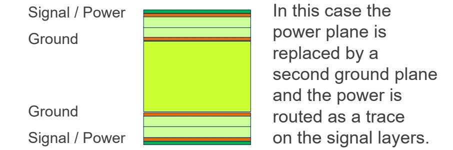
In this case, another ground plane is being used as the power plane, and power is routed as traces on the signal layers. This approach can enhance electromagnetic interference (EMI) performance, yet it does not offer shielding or isolation between different signal levels.
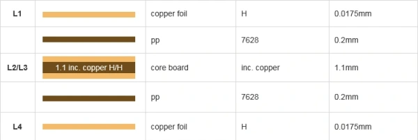
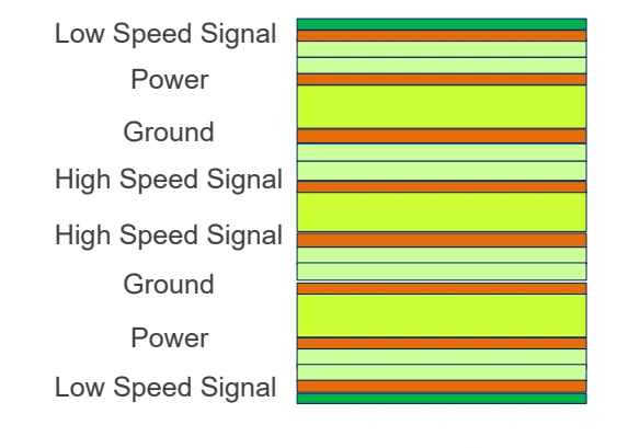
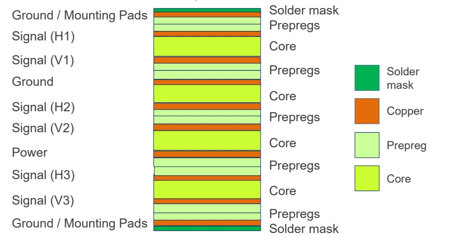
6-layer printed circuit boards are a suitable option when both cost and performance are significant factors. Here is a typical example of a frequent arrangement:
This arrangement effectively decreases electromagnetic emission by up to 10 decibels and offers excellent electromagnetic interference (EMI) performance through the utilization of high-speed communication between planes. Additionally, it diminishes susceptibility to external influences and offers electrostatic discharge (ESD) protection.
This configuration effectively separates the signal layers, minimizing interference and enhancing the quality of the signals. Ground planes serve the purpose of reducing noise and electromagnetic interference, while also functioning as channels for signal return.
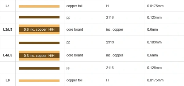

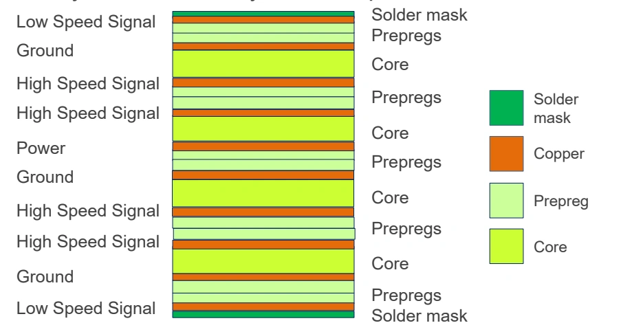
8-layer boards are commonly utilized when there is a need for enhanced performance. Typical stack-ups may consist of:
With its great EMI performance, low ground impedance, and effective shielding for high-speed communications, this topology satisfies all main design goals.
Another often-used 8-layer stack-up is shown here:
This configuration presents better power distribution and signal integrity. Apart from lowering electromagnetic interference, the extra ground planes offer fast transmissions with consistent reference planes.

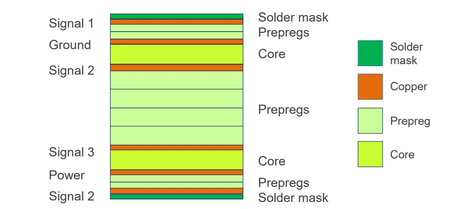
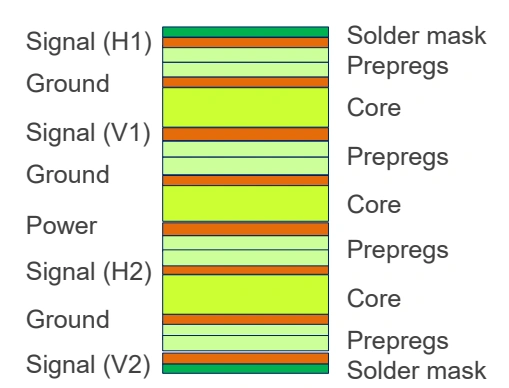
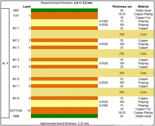
A 10-layer stack-up could be needed for the most demanding uses. Usually, a layout looks like this:
For systems requiring six routing layers, this stack-up provides exceptional signal layer shielding and isolation. It also reduces crosstalk by helping the orthogonal routing of signals next to the same plane, therefore improving signal integrity.
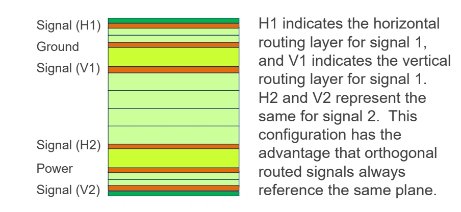
Another 10-layer configuration could be:
This setup is often found in top-tier communication and computing. It's popular because it guarantees strong signal quality and power supply.
1. Balance Signal and Power Layers: Make sure the base layers and energy source can back each other up. They need to have plenty of signal routes too. A good balance in design helps fix signal losses and power distribution issues.
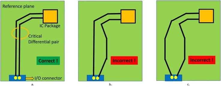
2. Minimize Crosstalk: Getting the best signal quality with the least amount of interference is our goal. To do this, place the signal layers near the ground planes. How? By using ground planes as guide layers and ensuring the right gap between signal traces.
3. Optimize Impedance: To meet the needs for impedance and crosstalk, you gotta be extra careful in measuring trace lengths, spacing, and die-electric thickness at the design stage. Utilizing pre-verified impedance control stackups is super important to keep a steady impedance in high-speed digital and radio frequency circuits. This stops signal reflection and distortion.
4. Thermal Management: To enhance heat dissipation, employ larger copper layers with ample spacing between them. Efficient thermal management is essential to ensure long-term reliability and prevent overheating of the PCB.
> Recommend reading: Fundamentals of PCB Thermal Design | NextPCB
5. Material Selection: Choose readily accessible materials with favorable electrical properties that satisfy assembly specifications. Material parameters such as loss tangent (Df) and dielectric constant (Dk) have a significant impact on signal integrity and should be carefully considered.
PCB stack design plans the board’s layer count, order, materials, and thicknesses to satisfy electrical, mechanical, and thermal requirements. A well-chosen stack couples signals tightly to stable reference planes, controls impedance to preserve signal integrity, provides stiffness and heat paths, and balances performance with cost. The process starts from system needs (speed, power, form factor), then converges on a layer sequence and material set, validated with electrical/thermal/mechanical checks and finalized with the fabricator for impedance control and tolerances.
Layer roles: signal routing; power/ground planes for distribution and reference; dielectrics to set impedance and isolate conductors; structural and thermal features for stiffness and heat spreading.
Why it matters: improves SI/EMI (lower crosstalk and loop radiation), ensures mechanical robustness, manages temperature, and optimizes cost.
Workflow (essentials): define requirements → pick layer count/ordering → choose materials & target dielectric thicknesses → simulate/verify → align with fab on stack, press-outs, and tolerances.
Practical tips: use the fewest layers that meet needs; favor stable, low-loss dielectrics (controlled Dk/Df); maintain copper balance and adequate thickness for flatness; add heat-spreading copper and thermal vias near hot zones; consider cost when selecting materials and thickness steps.
When designing a PCB layer stack-up, several things must be considered to meet requirements and optimize performance:
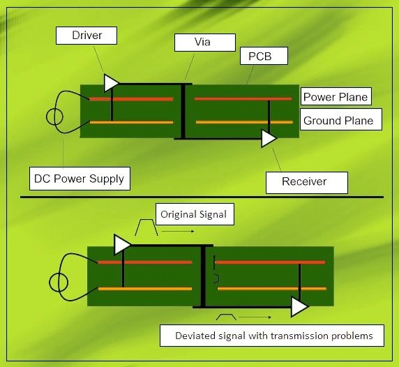
To preserve optimal signal integrity, it is imperative to strategically locate vias. These can vary in sorts, including buried, blind, and through-hole. Creating blind and buried vias might be challenging, but they are highly effective for conserving space and minimizing interference. On the contrary, through-hole vias are robust but can create challenges in routing for multi-layer systems. To maintain the quality of the signal, we can employ design techniques such as stitching or back-drilling. These components aid in regulating impedance and minimizing crosstalk. Thorough planning can enhance the functionality and dependability of printed circuit boards (PCBs) in intricate electronic systems.
> Recommend reading: HDI Via-in-Pad: Design, Fabrication, Reliability, and Performance
PCB Capabilities – 1–32 layers, rigid/flex/rigid-flex/HDI/metal-core, controlled impedance, blind/buried vias, via-in-pad, back-drill, multiple finishes (OSP, ENIG, HASL, Immersion Silver), tight trace/space, fine drills, and robust certifications (IPC Class 2/3 options, ISO/IATF/UL/RoHS/REACH).
PCB Prototypes – Fast-turn prototypes from single boards to small batches with online quoting and stackup guidance, bridging concept to pilot build.
PCB Assembly Services – Turnkey, consigned, or mixed SMT/BGA/THT assembly; 01005 passives, fine-pitch BGAs, X-ray and AOI inspection, functional testing, and rapid lead times.
BOM Services – Sourcing and optimization with cost/lead-time alternatives, lifecycle checks (EOL/NRND), and risk-mitigation substitutes.
Free DFM Check – Automated + engineer review for manufacturability (stackup, impedance, clearances, drills, solderability), returning actionable feedback before fabrication.
A critical step in PCB design involves the generation of PCB layer stack-ups. An optimized configuration of elements improves the electrical efficiency, durability, and ease of production of the final product. To meet the demanding criteria of contemporary electronic applications, PCB designers must have a thorough understanding of stack-up design principles and adhere to efficient approaches. Whether making a basic 4-layer board or a complex ten-layer one, the goal is managing different design goals and making smart compromises to get the best overall performance.
The world of PCB technology keeps evolving, allowing us to develop high-tech and compact electronic devices. Crafting reliable and unique electronics needs designers to excel at PCB layer stack-up, even when faced with fresh challenges and chances.

Still, need help? Contact Us: support@nextpcb.com
Need a PCB or PCBA quote? Quote now

