
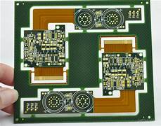
 NextPCB Capabilities
Printed Circuit Boards
NextPCB Capabilities
Printed Circuit Boards
 PCB Assembly
 Layer Buildup
 SMD-Stencils
 PCB Design-Aid & Layout
 Mechanics
 Quality
 Drills & Throughplating
 Factory & Certificate
 PCB Assembly Factory Show
Certificate
PCB Assembly Factory Show
Certificate
Support Team
Feedback:
support@nextpcb.com


Hi readers! I hope you are doing great. Today, we are talking about the manufacturing process of PCBs at home. Many of us think that manufacturing PCBs requires high skills and heavy machinery because of the large area where these PCBs can be designed and manufactured, but this is not the whole truth. Printed circuit boards require expertise and clear concepts about the structure of the PCB, and these can be easily manufactured at home. Although, Multilayer PCB is impossible to design at home.
In this article, we will start with the introduction of PCBs and then understand the steps to manufacture the PCBs at home. After that, we will learn the advantages of manufacturing PCBs at home and, in the end, see some limitations to doing so. Sopo, let us start with the introduction to PCB.
Most of us have seen or used printed circuit boards in our daily lives. These are used everywhere in electronics. We can say that without printed circuit boards, the concept of the electronic industry is something different. Here is the general definition of a PCB:
“A printed circuit board is a flat board made with non-conducting material. It has the conducting paths etched on the surface required for the conduction of current.”
It is a medium that is required for the connection of the wires in the circuit. The PCB is the fundamental component of modern electronics. This is the platform required for the connection and mounting processes of the electronic components in the circuit. As a result, these provide a strong foundation and help the circuit work properly without any fear of circuit deformation.
Manufacturing PCBs at home is a rewarding process, and most people prefer to manufacture these at home if they want PCBs on a small scale. This may be an easy process for those who have practised it or have seen it before. Multiple factors are responsible for the right manufacturing of PCBs, especially at home. Companies and other manufacturers have pre-defined parameters for each step, and one must have information about the whole process to manufacture the PCBs at home.
The manufacturing process of PCBs at home has almost the same steps as that of the companies that manufacture them. But the manufacturers at home use alternatives for the tools at some steps. Here, you can see that most of the tools are already present at home, so there is no need for a long preparation period for the manufacturing. So get all the material ready and follow the steps.
The first step is to make your creation live on software. There are multiple software programs used for the PCB design process, such as Proteus, KiCAD, Eagle, etc. Sometimes, students start making the PCB without any design and are stuck at the start because there is no mapping or reference.
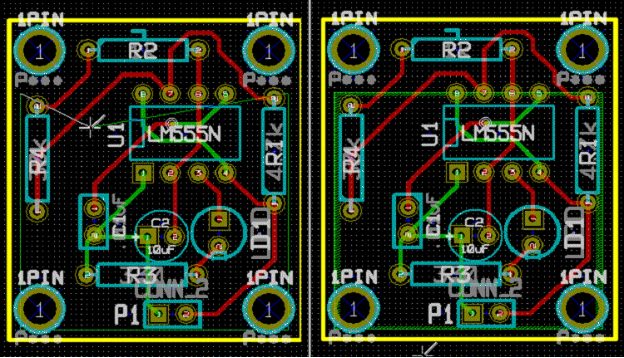
One must have a proper PCB layout design for the best results. Once the design is complete on the PCB software, it has to be printed on magazine paper or specialized transfer paper. For this, the computer system must be connected to the printer.
Before printing, make sure the print will have a high resolution and the design on it does not have any defects or mistakes. Moreover, the quality of the paper also matters in this case. The good thing is, it doesn’t matter if there was something else that was also printed on the paper; therefore, we also suggested the magazine paper for your convenience.
The board is prepared in this step, which means, there must not be any impurities on the surface. It is an important step, and we recommend that you use a steel or wool buffer so that the surface is shiny and lustrous. Moreover, sometimes the oxidation and contaminants are not visible on the surface, so don’t take any chances.
Place the printed design toner-sid down on the copper clad. Take care of the right placement and the alignment of the design with the cladding. Once the toner is placed perfectly, turn your clothing iron on at a high temperature. The printer toner starts melting at a high temperature, so make sure your iron is at the highest temperature but does not produce steam.
Place the hot iron on the backside of the printed layout for 30 seconds with full pressure. Try not to move the iron at this time. Now, move the iron slowly on the whole surface and apply full pressure without moving the cladding.
Once it is confirmed that the toner has been melted and transferred successfully, try to take off the paper. It will require some water. This step is crucial and requires high levels of patience and consistency. Drop the copper cladding into a tub of cold water. It will lower the temperature of the board and weaken the grip of the paper on the board.
This is the time to remove the paper manually. Try to peel the paper off. Try not to tear the paper, or don’t peel the paper so rapidly. If the toner is still stuck with the paper or is removed from the paper, it means the pressure applied with the hot iron is not enough. The previous step has to be repeated.
Wear the safety goggles and make the etching ready. Gloves are required in this step because the etching agent is usually reactive. Moreover, this step must be done in a highly ventilated area. Pour the etchant (usually ferric chloride) into a plastic tub, and we recommend you place the etchant in a warm place or in the sunlight for a rapid reaction rate.
This step takes 20-30 minutes, and the copper cladding has to be fully dipped into the etchant. The access copper will be dissolved in this way, leaving behind the design of the PCB in the form of toner.
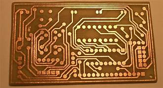
Once this step is completed, take the cladding off and dip it into the solution of water and soap to neutralise the etching present on the surface. Even after this, if a little copper is present on the cladding, remove it gently with a brush. As a result of this step, a clean, copper-free board will be there with only toner etched on it.
Use the steel wool or scrub again to remove the toner from the surface. After this step, the clean board with the copper design is seen on the board. Here, sometimes people use cutters to get the exact required size of their board.
Once again, look at the PCB design and start drilling the PCB. The places where there is a requirement for components are identified here. Use the small drip to make the holes for these components. Make sure you have a clear idea about all the components and the hole size because even a slight mistake at this point can ruin the whole board.
One must have knowledge of the hole size of the component presented in the specification details of that component. Gently apply pressure to the drill to make sure the board doesn’t break.
Now, your PCB is ready to assemble the components on it. The basic manufacturing of the PCB is completed here, but sometimes people require the whole assembly process as well and count it into the manufacturing, so let’s have a quick description of these steps.
Follow the PCB layout design and place all the components in their respective areas. It requires all the components to be together and nothing left because an incomplete circuit never works well. This is a crucial step, and make sure you place the components in their right position at once because inserting and removing the components can damage the pins or the board.
This is the most crucial step and has to be done carefully. Never test an incomplete board because it can harm the circuitry. Once you are sure that all the components are placed in the perfect position, try to test the circuit by taking precautionary measures. It is recommended to check the soldering, shorts, or any other errors before testing. Now, power up the circuit to test it.
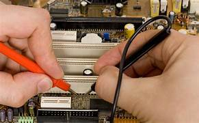
The testing requires simple parameters to be met. Check each component in different possible ways. Check the behaviour of each component with different tools, such as the multimeter, etc. If all goes well, you will have made a perfect PCB at home.
There are multiple advantages to manufacturing the PCB at home instead of going to a company for the whole process. Some of these are known to all users, but we have made a list to highlight the importance of manufacturing them themselves. Here is the list with descriptions:
One of the most highlighted advantages of doing so is the cost of PCB manufacturing. If you have the skill to design and manufacture your own PCB, then this is the best option. Usually, companies have a limit on minimum orders on the board, and if this does not match the number of PCBs the customer needs, they are not able to work for them. Hence, it is a cost-effective idea to manufacture your own PCBs.
During the manufacturing of PCBs, all the controls are in the hands of the manufacturer. If someone decides to manufacture their own PCB, they can easily customize all the features without any problem. Many times, the customers are not able to express all the requirements, but the specific designing can be done by themselves on the PCBs.
The time to order the PCB, make the design clear, and wait for the company to manufacture it is too much for small orders. On the other hand, if these are manufactured at home, it takes very little time. As you can see, the above steps are not complicated and take little time.
Manufacturing the PCB gives you the freedom for live troubleshooting. The testing process is done on your own so that issues are encountered at the initial level. Checking and identifying the issues is easy in this way.
There are many advantages to manufacturing the PCB at home, but it is not suitable for all types of PCBs. Here are some of the limitations and disadvantages of doing so:
Hence, we have read the detailed step-by-step guide to manufacturing PCBs at home. We have read about the process with all the equipment. Moreover, we have seen the advantages of manufacturing these at home and have learned about the limitations as well. I hope you have understood it well but never forget to follow the precautionary measures.
New Automated PCB Assembly Quotation System - Order in Just a Few Steps! (Blog)
How to Order PCB & PCBA from NextPCB? (Blog)
How to place a PCBA order? (FAQ)
How long is the lead time for PCB Assembly (PCBA) orders? (Blog)
PCB Assembly (PCBA) FAQ
Still, need help? Contact Us: support@nextpcb.com
Need a PCB or PCBA quote? Quote now


 Surface

