Introduction
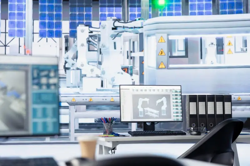
The Fourth Industrial Revolution is reshaping how factories, supply chains, and critical infrastructure operate. At the heart of this transformation lies the Industrial Internet of Things (IIoT)—a powerful convergence of sensors, machines, and networks that enables real-time data collection, intelligent decision-making, and unprecedented levels of automation. Unlike consumer IoT, which focuses on convenience in daily life, IIoT is built to power mission-critical operations where failure is not an option.
This shift introduces a new battlefield for hardware design. Industrial environments demand equipment that can withstand extreme temperatures, constant vibration, electromagnetic interference, and decades of continuous operation. For engineers, this means designing industrial-grade systems that go far beyond scaling up consumer electronics. Every design decision—from chip selection and PCB layout to thermal management and shielding—directly influences system reliability, safety, and long-term cost efficiency.
This blog explores the essence of IIoT hardware design, the challenges engineers face in harsh industrial settings, and the strategies that ensure resilience, efficiency, and scalability. By examining the interplay of materials science, mechanical engineering, and electronics, we’ll see how thoughtful design choices lay the foundation for the next generation of smart manufacturing.
From NextPCB’s perspective, meeting these industrial requirements means upgrading materials and processes across the board—supporting high-Tg laminates, Rogers and ceramic substrates, metal-core boards, thermal-via arrays and thicker copper, plus robust DFM/assembly workflows and automated inspection (AOI/AI-assisted QA)—so designs for IIoT can be translated rapidly and reliably from prototype to high-volume production.

Table of Content:
- Part I: The New Battlefield for IIoT Hardware Design
- Part II: Challenge 1 — High Temperatures
- Part III: Challenge 2 — Vibration and Shock
- Part IV: Challenge 3 — Electromagnetic Interference (EMI)
- Part V: System Integration and Future Outlook
- Conclusion
Part I: The New Battlefield for IIoT Hardware Design
1.1 The Essence of IIoT: A Paradigm Shift from "Consumer-Grade" to "Industrial-Grade"
The Industrial Internet of Things (IIoT) is a core component of the Fourth Industrial Revolution. At its essence, it connects physical devices, sensors, robots, and industrial assets to a network to collect and exchange data. This enables advanced applications like automation, remote monitoring, and predictive maintenance. Unlike the consumer-grade Internet of Things (IoT) found in smart homes and wearables, IIoT isn't just a matter of scaling up; it's a "system of systems" architecture that deeply integrates devices, systems, and the cloud. Its core value lies in using real-time data insights to optimize production processes, enhance efficiency and accuracy, reduce operational costs, and maximize production safety.
The fundamental differences between IIoT and consumer IoT are reflected in the stringent requirements of the "Five -ilities," which directly shape the unique characteristics of IIoT hardware design:
- Reliability: In consumer IoT, a malfunctioning smart thermostat may just be an inconvenience, but in an IIoT environment, device downtime can have severe consequences. For example, a sensor failure could lead to a toxic gas leak, or a smart grid outage could affect an entire city. Therefore, the pursuit of reliability in IIoT is a fundamental driver of design decisions.
- Scalability: In consumer IoT, scalability challenges are usually cloud-centric, focused on how to handle millions of user data requests simultaneously. In contrast, IIoT scalability lies mainly at the "edge," where real-time communication with hundreds of machines and thousands of sensors must be sustained.
- Latency: IIoT applications like industrial control, robotic collaboration, and precision manufacturing require performance and latency in the millisecond range to ensure real-time decision-making and high-precision operations. This is far beyond the second-level latency tolerated by consumer IoT.
- Heterogeneity and Interoperability: Industrial environments often consist of equipment with diverse technical standards, ranging from traditional devices that have been operating for decades to newly deployed smart machines, which often lack a unified communication protocol. IIoT systems must have powerful capabilities to handle this heterogeneity and interoperability, seamlessly connecting these "data silos" and integrating efficiently with legacy systems.
- Upgradability: Consumer IoT devices typically have short lifespans, but in industrial environments, expensive equipment is expected to run for years or even decades. Therefore, IIoT hardware must be designed from the outset with an architecture that is repairable, upgradable, and extensible, supporting remote firmware updates to meet future challenges and technological evolution.

1.2 Industrial-Grade Components: The Bedrock of Reliability
The demand for reliability and durability in IIoT fundamentally dictates the choice of core components. Industrial-grade chips differ significantly from common consumer-grade chips in design, manufacturing, and performance metrics, which allows them to operate reliably in harsh environments.
1.2.1 Key Differences and Critical Metrics
Industrial-grade chips are designed for fields such as factory automation, robotics, and medical devices, and their key metrics are typically much higher than those of consumer-grade chips.
- Operating Temperature Range: Consumer-grade chips typically operate from 0∘C to 70∘C, while industrial-grade chips must adapt to a wider range, usually from −40∘C to 85∘C or higher. For more extreme applications like aerospace or car engine compartments, components may operate from −55∘C to 125∘C or even wider.
- Reliability Standards: Industrial-grade components follow industry standards like JESD47, while automotive-grade components adhere to the even stricter AEC-Q100 standard. These standards ensure high reliability and durability during the design and manufacturing processes.
- IC Failure Rate and Lifespan: Industrial-grade chips undergo stringent qualification, typically resulting in significantly lower FIT (Failures In Time) rates and longer MTBF (Mean Time Between Failures). For example, lifespans of ~10 years are common under typical operating conditions.
- Environmental Resilience: Industrial-grade components have greater resistance to vibration, humidity, and salt spray, which is critical for ensuring long-term stable operation in harsh physical environments.
The following table provides a clear comparison of key differences between industrial-grade and consumer-grade components:
|
Characteristic
|
Consumer-Grade Chip
|
Industrial-Grade Chip
|
Automotive-Grade Chip
|
|
Typical Operating Temperature
|
0∘C to 70∘C
|
−40∘C to 85∘C or higher
|
−40∘C to 125∘C
|
|
Reliability Standards
|
No strict standards
|
JESD47
|
AEC-Q100
|
|
IC Failure Rate
|
No strict definition
|
<1%
|
Extremely low (AEC-Q100 qualified)
|
|
Typical Lifespan
|
A few years
|
~10 years
|
~15 years
|
|
Environmental Resilience
|
Relatively weak
|
High, resists vibration, humidity, salt spray
|
Extremely high, must meet vehicle safety standards
|
|
Typical Applications
|
PCs, phones, home appliances
|
Robotics, automation, medical equipment
|
Engine control, driver-assist systems
|
1.2.2 The Deeper Trade-off Between Cost and Reliability
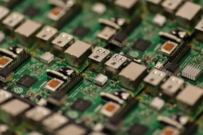
In the early stages of an IIoT project, designers might be attracted by the low initial cost of consumer-grade chips, as low-cost kits like Raspberry Pi and Arduino are ideal for rapid prototyping. However, this is a short-sighted cost consideration. Although the initial cost of industrial-grade components may be several times higher, their wider operating temperature range, lower failure rate, and longer lifespan will significantly reduce the Total Cost of Ownership (TCO) and ensure production continuity.
This choice reflects a results-oriented design mindset: every device downtime caused by component failure means expensive repair costs and potential safety risks. In an industrial environment, the loss from an hour of production line downtime can far exceed the value of a single piece of equipment. Therefore, choosing industrial-grade components is not a luxury but a necessary investment to avoid future massive losses due to failures. This comprehensive trade-off, based on the product's full lifecycle and potential failure costs, is the core principle that distinguishes IIoT hardware design from consumer electronics design.
1.3 The Three Core Challenges of Industrial-Grade PCB Design
In the landscape of IIoT hardware, the PCB serves as the central carrier for all components, making its reliability paramount. The industrial environment poses three core challenges to PCBs: high temperatures, vibration and shock, and electromagnetic interference (EMI). This report will delve into each of these three challenges and provide systematic solutions, aiming to offer engineers and designers an authoritative and practical technical guide.
Part II: Challenge 1: High Temperatures, The Invisible Performance Killer
High temperatures in industrial environments refer not only to the heat generated inside the equipment but also to the extreme temperatures of the external environment, such as next to a high-temperature furnace on a factory floor or direct sunlight on outdoor equipment. This thermal stress poses a serious threat to PCB reliability.
2.1 How High Temperatures Damage PCBs
PCB failure in high-temperature environments is a result of a combination of physical and chemical effects.
- Coefficient of Thermal Expansion (CTE) Mismatch: The materials that make up a PCB, such as the substrate (FR-4), copper traces, and solder, have different CTEs. For example, the CTE of FR-4 is about 16−17 ppm/∘C, while that of copper is 16.5 ppm/∘C. Although these differences seem minor, they create cumulative mechanical stress, especially at solder joints and through-hole regions, during repeated thermal cycles (e.g., power on/off or environmental temperature changes). This stress is the fundamental cause of solder joint fatigue cracking, board delamination, and warping.
- Chemical and Physical Changes: High temperatures accelerate metallurgical changes in solder alloys (e.g., tin-silver-copper), weakening joint structure. In humid and voltage-present environments, high temperatures can accelerate the process of "electrochemical migration," where metal ions move between conductors, forming dendrites that eventually lead to short circuits.
- Component Performance Degradation and Shortened Lifespan: The electrical parameters of components (e.g., resistance, capacitance) drift as temperature increases, affecting the normal operation of the circuit. Furthermore, long-term exposure to temperatures outside their rated range can significantly shorten a component's expected lifespan, increasing the risk of failure.
2.2 PCB Material Selection: A Dual Consideration of Heat Resistance and Thermal Conductivity
To address the high-temperature challenge, PCB design must be optimized from the perspective of material selection, which requires considering both the substrate's heat resistance and its ability to conduct heat.
2.2.1 High-Tg Materials: The Foundation of Heat Resistance
The glass transition temperature (Tg) is the critical temperature at which a substrate material transitions from a rigid, glassy state to a soft, rubbery state. Once Tg is exceeded, the material's mechanical strength and electrical performance degrade significantly. Therefore, in high-temperature environments, materials with a higher Tg value must be chosen. Industrial-grade designs typically recommend using high-Tg PCBs, with Tg values usually equal to or greater than 170∘C. Compared to traditional FR-4 (with a Tg of about 130−150∘C), high-Tg materials offer the following advantages:
- Higher Dimensional Stability: Better at maintaining size and shape at high temperatures.
- Stronger Delamination Resistance: Effectively resists delamination caused by thermal stress.
- Lower Z-axis CTE: Reduces thermal expansion in the vertical direction (Z-axis), protecting the reliability of plated through-holes (PTHs).
High-Tg materials are particularly suitable for multilayer boards and high-density interconnect (HDI) boards because these boards have dense internal circuitry and are more prone to heat buildup. Common industrial-grade high-Tg materials include Isola 370HR (180∘C) and Panasonic R1755V (175∘C), as well as the Rogers RO4000 series (Tg up to 280∘C) designed for high-frequency applications.
2.2.2 High-Efficiency Thermal Substrates: Ensuring Rapid Heat Dissipation
In addition to heat resistance, the thermal conductivity of the PCB is also crucial. Heat generated by high-power components needs to be quickly conducted and dissipated to avoid localized hot spots.
- Metal-Core Substrates: Metal substrates with an aluminum or copper core have much higher thermal conductivity than FR-4. Aluminum substrates, due to their high cost-effectiveness and light weight, are often used in LED lighting and high-power supply equipment.
- Ceramic Substrates: Ceramic materials (e.g., Al2O3, AlN) offer 9–20 W/mK thermal conductivity and a CTE closer to copper, thereby reducing thermomechanical stress. This makes them ideal for a new generation of large-scale integrated circuits. It's worth noting that silicon carbide (SiC) has very high thermal conductivity, in the range of ~120–270 W/mK, depending on form and processing method, and performs excellently in high-power or high-temperature applications.
The table below compares the key characteristics of common industrial-grade PCB substrate materials:
|
Material Type
|
Glass Transition Temperature (Tg)
|
Coefficient of Thermal Expansion (CTE)
|
Thermal Conductivity (TC)
|
Dielectric Constant (Dk)
|
Dissipation Factor (Df)
|
Typical Applications
|
|
Standard FR-4
|
130−150∘C
|
Medium ( 17 ppm/∘C)
|
Low (0.25 W/mK)
|
Medium ( 4.5)
|
Medium ( 0.015)
|
General IIoT devices, consumer electronics
|
|
High-Tg FR-4
|
≥170∘C
|
Lower ( 14 ppm/∘C)
|
Lower
|
Medium ( 4.2)
|
Lower ( 0.010)
|
Multilayer boards, HDI, automotive electronics
|
|
Polyimide
|
≥250∘C
|
Extremely low
|
Low
|
Lower ( 3.8)
|
Extremely low ( 0.005)
|
Aerospace, military, flexible circuits
|
|
Rogers
|
≥280∘C
|
Extremely low
|
Lower ( 0.5 W/mK)
|
Extremely low (3-6.5)
|
Extremely low ( 0.002)
|
High-frequency RF, microwave comms, 5G
|
|
Metal-Core Substrate
|
Not applicable
|
High
|
Extremely high (>10 W/mK)
|
Not applicable
|
Not applicable
|
High-power LEDs, power modules, automotive
|
|
Ceramic Substrate
|
Extremely high
|
Extremely low ( 8 ppm/∘C)
|
High (9−20 W/mK)
|
Higher (>10)
|
Extremely low
|
High-performance IC packaging, specialized sensors
|
2.3 Thermal Management Design Techniques: Active and Passive Heat Dissipation
Relying solely on material properties is not enough; excellent thermal management requires combining material selection with clever PCB layout and pcb design techniques.
2.3.1 PCB Layout Optimization
- Heat Source Partitioning: Segregate high-heat-generating components (e.g., processors, power devices) from heat-sensitive ones (e.g., sensors, analog circuits) to prevent heat from affecting each other.
- Thermal "Pizza Slice" Model: Heat conduction on a PCB is not uniform; it radiates outward from the heat source in a "pizza slice" pattern. Therefore, in the vicinity of a heat source, avoid traces or ground plane cuts to ensure the continuity and unimpeded flow of the thermal conduction path.
> Expand reading: PCB Thermal Design Basics (2): Component Layout
2.3.2 Building High-Efficiency Thermal Conduction Paths
- Copper Planes: Copper has a thermal conductivity of about 385 W/mK, which is much higher than FR-4's 0.25 W/mK. Therefore, using large copper planes on the top and bottom layers as heat sinks is the primary strategy for reducing thermal resistance. Increasing the number of PCB layers (e.g., from 2 to 4 or more) and increasing copper thickness (e.g., from 1 oz/ft2 to 2 oz/ft2) can significantly enhance overall heat dissipation.
- Thermal Vias: Thermal vias are highly efficient vertical thermal conduction channels that connect copper planes on different layers. Placing an array of thermal vias directly under the Die Attach Pad (DAP) of a heat-generating component can quickly conduct heat from the source to internal copper layers or to a heat sink on the backside. Thermal via diameter, annular ring width, and spacing will vary significantly depending on the process, board thickness, and thermal resistance goals. It is generally recommended to use 12-mil diameter thermal vias and ensure a sufficient quantity to maximize the reduction in total thermal resistance. Furthermore, common practices include using vias filled with thermally conductive material or using blind/buried vias to further optimize thermal conduction and reduce thermal resistance.
2.4 Critical Analysis: A Systematic Approach to Thermal Management
PCB thermal management is a multi-level, multi-dimensional system engineering task, not just the application of a single technique. Heat starts at the junction temperature (TJ) inside the chip, is transferred through the package to the PCB, and then conducted through the copper planes and thermal vias on the PCB to the external environment. This process forms a complete "thermal resistance chain":
RTotal=RJC+RCP+RPA
Where RJC is the junction-to-case thermal resistance, RCP is the case-to-PCB thermal resistance, and RPA is the PCB-to-ambient thermal resistance.
A bottleneck in any one of these links will affect the overall heat dissipation effect. For example, even if a substrate with excellent thermal performance is selected, if the layout is improper and heat cannot be effectively conducted to a large copper plane, the final heat dissipation effect will still be poor. Therefore, designers must perform a global optimization of chip selection, package design, PCB layout, material selection, and external heat dissipation solutions to ensure the long-term reliability of the product in extreme temperatures.
Part III: Challenge 2 — Vibration and Shock, The Relentless Test of Mechanical Stress
In industrial settings, equipment is exposed to constant mechanical vibration (e.g., from engines, motors) or sudden shocks (e.g., from transport bumps, accidental collisions) year-round. These mechanical stresses are another major cause of PCB hardware failure.
3.1 How Vibration and Shock Destroy PCBs
The damage caused by mechanical stress to PCBs is both insidious and cumulative.
- Solder Joint and Trace Fatigue Cracking: Continuous vibration can cause the PCB to bend and deform, putting repeated mechanical stress on solder joints, component leads, and copper traces. Over time, this leads to the initiation and propagation of microcracks, eventually causing fatigue failure. This is particularly true for BGA and leadless SMT components, which are highly sensitive to board bending due to their large pad area and lack of flexible leads, making them prone to solder joint cracking.
- Component Detachment and Connection Interruptions: Severe vibration may cause solder joint fractures or complete detachment of heavy/tall components. Connectors may also become loose during vibration, leading to momentary or permanent contact failure.
- Mechanical Resonance: When the external vibration frequency matches the natural resonant frequency of the PCB board or its components, it can cause a resonance effect. This can rapidly amplify stresses and cause catastrophic failure if not mitigated.
3.2 PCB Anti-Vibration Design Strategies
Excellent anti-vibration design requires a systematic approach from multiple levels.
Board Material and Thickness: Increasing the rigidity of the PCB is an effective way to resist vibration stress. Using a thicker PCB (e.g., 2.0mm or more) can effectively reduce board bending, thereby reducing stress on components and solder joints. Additionally, selecting high-strength, high-Tg board materials, such as high-Tg FR-4 or polyimide, can enhance the board's mechanical stability under thermal stress.
Component Layout and Reinforcement:
- Strategic Layout: Place heavy or stress-sensitive components (e.g., BGAs, ceramic capacitors) in low-strain areas of the PCB, such as near mounting holes or board edges. Avoid placing these components in long-span or high-stress areas (e.g., the center of the board).
- Use of Adhesives: For critical or heavy components, use underfill, adhesives, or reinforcing brackets to securely fix them to the PCB, preventing movement or detachment during vibration.
- Multi-Point Support and Vibration Isolation:
- - Multi-Point Fixing: Using multi-point support can evenly distribute mechanical stress. For example, evenly distribute multiple mounting points at the four corners and center of the board, avoiding long unsupported spans.
- - Vibration-Isolating Mounts: Use vibration-isolating materials like silicone pads, rubber damping pads, or spring mounts to isolate the PCB from the equipment's chassis. These materials can effectively absorb and attenuate the vibration energy transmitted to the circuit board, significantly reducing vibration stress.
- Connectors and Interfaces: Choosing connectors specifically designed for harsh environments is crucial. These connectors typically have the following characteristics:
- - Locking Mechanisms: To prevent loosening or detachment during vibration.
- - High-Durability Contacts: Use corrosion- and wear-resistant materials like gold plating to ensure long-term reliable electrical connection.
- - Tolerance Compensation: With floating functions or insertion chamfers that can compensate for small displacements of the PCB during vibration, preventing contact wear and connection interruptions.
3.3 Critical Analysis: A Systematic Consideration of Physical Protection
PCB anti-vibration design is a "mechatronics" system engineering task that goes beyond the scope of pure electronics design, requiring designers to have a mechanical engineering mindset. The failure path is a complete physical chain: vibration is first generated from the external environment (e.g., an engine), transmitted through the equipment chassis to the PCB's mounting points, and then the PCB's rigidity, thickness, layout, and mounting method determine how this mechanical stress is distributed and attenuated on the board, ultimately acting on the solder joints and components themselves.
Therefore, a truly excellent anti-vibration design must perform full-chain optimization from the vibration source (via isolation), the conduction path (via chassis rigidity, multi-point support), and the final stress points (via board material selection, layout optimization, and component reinforcement). A weakness in any single link can lead to the failure of the entire system. This is a physical-level systematic consideration that requires engineers to closely integrate PCB design with the overall mechanical structure design of the product to provide a solid guarantee for the long-term reliability of IIoT equipment in harsh environments.
Part IV: Challenge 3 — Electromagnetic Interference (EMI)), The Hidden Danger in Complex Signal Environments
In industrial environments, high-speed switches, high-power motors, and wireless communication devices are all major sources of electromagnetic interference (EMI). This electromagnetic noise can severely affect a device's signal integrity and functional stability.
4.1 The Roots and Harms of EMI
- Generation Mechanism: The root cause of EMI is the time-varying current on conductors, i.e., di/dt noise. When current changes rapidly, it generates electromagnetic field radiation. In some cases, PCB traces can act like antennas, radiating this electromagnetic energy. For example, if a high-speed signal crosses a ground plane split, its return current is forced to detour, creating a large current return loop and causing serious radiation.
- Dual Harm: EMI has a dual harm. First, the radiation generated by the device itself can interfere with other devices, causing them to malfunction. Second, the device can also receive electromagnetic interference from the outside, and this energy couples into sensitive traces, leading to signal distortion, data errors, and even device function failure.
- The Dialectical Relationship between "Spear" and "Shield": A good "antenna" (i.e., an efficient radiation source) is also a good "receiver" (i.e., a sensitive receiver). Therefore, EMI design for PCBs is both an active "offense" (reducing self-radiation through design optimization) and a passive "defense" (resisting external interference through shielding and filtering). These two functions are two sides of the same coin, and techniques that suppress radiation usually also enhance anti-interference capability.
4.2 PCB Layout and Routing: Suppressing EMI at the Source
From a layout perspective, EMI is fundamentally about managing current flow and minimizing antenna structures. Suppressing EMI at the source is the most important part of PCB design.
- Ground Plane Design: In multilayer boards, using one or more solid ground planes is crucial. A solid ground plane not only provides a low-impedance common return path for all signals but also effectively acts as a shield, suppressing the radiation of internal noise. Designers should absolutely avoid unnecessary cuts in the ground plane, especially under high-frequency signal traces.
- Signal Tracing Techniques:
- Routing Rules: Avoid 90° right-angle traces, which introduce impedance discontinuities and radiate more strongly. Use 45° bends or arcs instead.
- Minimize Return Loop Area: This is a core principle of EMI design. High-frequency signals must always be routed close to their return path (usually an adjacent reference ground plane), and the loop area between the two should be minimized as much as possible.
- Differential Pair Routing: For high-speed differential signals, the two traces must be routed with strict length matching and constant spacing, to maintain differential impedance and strong noise immunity.
- Functional Partitioning: Physically partitioning analog circuits, digital circuits, radio frequency (RF) circuits, and power circuits on the PCB and isolating them on the ground plane can effectively prevent high-frequency digital noise from coupling into sensitive analog and RF circuits.
4.3 EMI Mitigation and Shielding Techniques
Besides layout and routing, additional techniques can be used to further mitigate EMI issues.
- - Shielding Cans: Use metal shielding cans for sensitive or high-noise circuits (e.g., RF modules, clock sources) to form a "Faraday cage," which effectively confines electromagnetic energy.
- - Ground Pouring and Stitching: Filling idle areas of the PCB with copper and connecting it to the ground plane creates a "shielding wall," which further suppresses radiation. In multilayer boards, using "stitching vias" to connect different ground planes at the board's edge forms a continuous, closed shielding structure that contains internal signal radiation.
- Filtering and Decoupling:
- - Decoupling Capacitors: Placing decoupling capacitors near an IC's power pins provides a low-impedance bypass path, shunting high-frequency noise directly to the ground plane and minimizing the power return loop.
- - Ferrite Beads: Ferrite beads in series with power lines act as high-frequency noise "absorbers" or low-pass filters.
Part V: System Integration and Future Outlook

5.1 The Integrative Mindset and Key Trade-offs in IIoT Hardware Design
High temperatures, vibration, and EMI aren't isolated challenges; they are interconnected and require designers to make complex trade-offs. For example, while thicker copper layers improve thermal management, they can alter impedance profiles of high-frequency traces, increasing EMI risk.
Designers must have an integrative mindset and make trade-offs in the following key dimensions:
- - Performance vs. Cost: High-performance materials like Rogers and ceramics offer excellent electrical and thermal properties, but their cost is high. High-Tg FR-4 provides a better balance between performance and cost.
- - Thermal Management vs. Size: The trend toward miniaturization in IIoT equipment means more heat is generated in a smaller area. This requires designers to find the best balance between High-Density Interconnect (HDI) design and efficient heat dissipation, for example, by using micro-vias and optimized thermal paths.
5.2 Legacy Systems and Future Upgradability
In industrial environments, a significant challenge is integrating legacy systems that lack modern connectivity standards. Edge computing provides a solution by deploying intelligent gateways to translate old protocols and extract valuable data.
However, a forward-thinking design anticipates that today's IIoT devices will become the new "legacy systems." Therefore, a responsible design must consider the product's full lifecycle and build a system that supports upgradability, remote firmware updates, and a robust security architecture. This includes implementing strong authentication, encrypted communication, and regular updates to counter evolving cyber threats.
Conclusion: Laying a Solid Foundation for Smart Manufacturing
The Industrial Internet of Things is a core driver for smart manufacturing. Its success depends not only on software innovation but also on a solid hardware foundation. This article has detailed the three core challenges—high temperatures, vibration, and EMI—and provided comprehensive solutions from material selection and PCB layout to component reinforcement and a systematic design mindset.
IIoT hardware designers are like architects for the future smart world, building a digital highway that must be sturdy enough to resist harsh environments, efficient enough to transmit massive real-time data, and secure enough to withstand unknown attacks. This requires them to combine expertise from materials science, mechanical engineering, thermodynamics, and electromagnetism.
At NextPCB, a one-stop pcba manufacturer, we understand the stakes. We have fundamentally enhanced our services to meet these rigorous demands. We've upgraded our material procurement channels, ensuring we stock a wide range of industrial-grade and specialty substrates like high-Tg FR-4, Rogers, and ceramic-core boards. Our manufacturing processes have been optimized for extreme reliability, with tighter controls over thermal dissipation via layouts with thermal vias, robust component mounting to resist vibration, and specialized shielding techniques to combat EMI. Our automated quality assurance has been significantly improved, providing unprecedented consistency and reliability for every board. We've invested heavily so that our engineers and our state-of-the-art facilities can handle the toughest challenges. The next generation of PCBs will determine the future of Industry 4.0, and NextPCB is ready to partner with you to build that future.
|
Core Challenge
|
Main Failure Modes
|
Preferred Materials
|
Design Strategies
|
|
High Temperatures
|
Solder joint fatigue, board delamination, shortened component lifespan
|
High-Tg FR-4, polyimide, metal-core substrates, ceramic substrates
|
Thermal via arrays, large copper planes, heat source partitioning, external heat dissipation solutions
|
|
Vibration and Shock
|
Solder joint cracking, component detachment, mechanical resonance, trace breakage
|
High-Tg FR-4, polyimide, thick board (>2.0mm)
|
Multi-point support, component reinforcement, vibration-isolating mounts, strategic layout
|
|
Electromagnetic Interference (EMI)
|
Signal distortion, data errors, device malfunction
|
Low Dk/Df materials (e.g., Rogers), solid copper planes
|
Minimize return loop area, avoid ground plane splits, functional partitioning, use shielding cans
|
About the Author
Sylvia joined NextPCB two years ago and has already become the go-to partner for clients who need more than just boards. By orchestrating supply-chain resources and refining every step from prototype to mass production, she has repeatedly delivered measurable cost savings and zero-defect launches. Consistency is her hallmark: every client, every order, receives the same uncompromising quality and responsive service.


 NextPCB Capabilities
 PCB Assembly
 Layer Buildup
 SMD-Stencils
 PCB Design-Aid & Layout
 Mechanics
 Surface
 Quality
 Drills & Throughplating
 Factory & Certificate