

 NextPCB Capabilities
 PCB Assembly
 Layer Buildup
 SMD-Stencils
 PCB Design-Aid & Layout
 Mechanics
 Surface
 Quality
 Drills & Throughplating
 Factory & Certificate


Printed Circuit Boards (PCBs) are the heart of modern electronic devices. Their performance, reliability, and ultimate function are not determined solely by the circuit design but, more fundamentally, by the materials used. From handheld mobile devices to complex aerospace systems, the choice of PCB material is a critical engineering decision that directly impacts the product's electrical performance, thermal management capabilities, and long-term durability. Selecting the wrong material can lead to signal integrity issues, thermal runaway, and even product failure, while the right material can unlock the full potential of a design.
This guide is intended to be a comprehensive and authoritative resource on PCB materials. It systematically explains everything from basic classifications to the subtle properties of high-performance laminates, providing practical selection criteria for modern applications.
I. PCB Construction: Understanding the Basic Building Blocks
To understand the importance of PCB materials, one must first analyze their fundamental construction. A typical PCB is composed of multiple stacked layers, with each layer using a specific material to fulfill its function.
> Recommend reading: Why Is the Option of Selecting the Count of Layers Mostly Even?
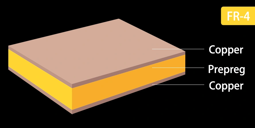
1. The Substrate: The Skeleton of the Board
The substrate is the physical skeleton of the PCB, providing mechanical support and electrical insulation for all electronic components. It is a composite material made of a reinforcing material and a resin binder. The reinforcing material is usually glass fiber cloth or paper, while the resin can be of various types, such as epoxy resin. The choice of substrate is the most diverse part of the entire PCB manufacturing process and the one that best reflects customer customization needs.
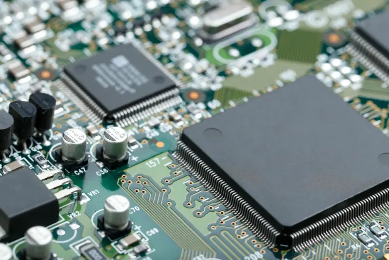
2. The Conductive Layer: The High-Speed Highway for Signals
The conductive layer is a thin layer of copper foil laminated onto the substrate to form electrical traces, pads, and planes. This copper foil serves as the channel for electronic signals. For high-performance applications, the type and treatment of the copper foil are also critical. For example, Reverse Treated Copper can improve its adhesion in complex multilayer designs, while Resistive Foil helps achieve advanced impedance control.
3. Solder Mask and Silkscreen: Protection and Identification
In addition to the core substrate and copper foil, a PCB also has outer layers for protection and identification. The Solder Mask is an insulating coating that covers the copper traces to prevent short circuits and protect the circuit from environmental factors. The Silkscreen layer provides component markings, reference designators, and company logos on the board, which is useful for assembly and repair. Together, these materials ensure the reliability and usability of the PCB.
> Recommend reading: PCB Assembly - The Most Comprehensive Guide | NextPCB
II. PCB Material Classification: A Comprehensive Analysis
Classifying PCB materials helps designers and manufacturers systematically select the appropriate base material for different application requirements. These classifications are typically based on their physical and chemical properties.
1. Classification by Base Material Type
- FR-4 (Epoxy Glass Cloth): FR-4 is the most popular standard base material in the industry. It is composed of woven glass cloth reinforced with flame-retardant epoxy resin. FR-4 is known for its excellent mechanical strength, electrical performance, and heat resistance, and is widely used in consumer electronics and industrial equipment.
- Paper-based Laminates (FR-1, FR-2): These materials are mainly made of paper and phenolic resin. They are low-cost and typically used for simple single-sided boards in general consumer electronics. They have good flame retardancy (FR-1, FR-2 are flame-retardant grades) and are suitable for punching at temperatures between 40°C and 70°C.
- Composite Laminates (CEM-1, CEM-3): Composite materials are designed to combine the advantages of paper-based and glass cloth-based laminates. CEM-1 has a paper core with glass cloth on the outer layers, while CEM-3 has a mixed core of woven glass cloth and non-woven glass fiber. They combine the easy processability of paper-based boards with the superior mechanical and dielectric properties of glass cloth boards, making them suitable for applications where both cost and performance are a consideration.
- Specialty Laminates: In addition to these common types, there are special laminates for specific applications, such as metal-core substrates for thermal management and ceramic substrates for high-frequency applications.
2. Classification by Resin Type
The resin in PCB materials is a key factor that determines their electrical, thermal, and mechanical properties.
- Phenolic Resin (FR-2): A low-grade material typically used for single-sided boards with limited durability.
- Epoxy Resin (FR-4 Series): Features excellent mechanical and electrical properties with good heat resistance and is widely used.
- Polyimide (PI) Resin: Offers outstanding high-temperature resistance, making it suitable for electronic devices operating in extreme thermal environments.
- Polytetrafluoroethylene (PTFE or Teflon): Known for its excellent high-frequency performance and is the preferred choice for antenna and radio frequency (RF) applications.
- Bismaleimide Triazine (BT): Has higher heat resistance and dimensional stability, making it ideal for multilayer PCBs.
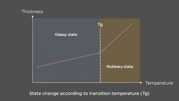
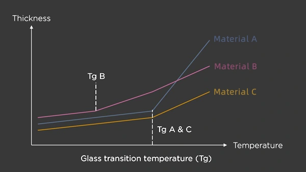
3. Classification by Glass Transition Temperature (Tg)
Tg is the temperature at which a PCB material transitions from a rigid, glassy state to a pliable, softened state. A higher Tg value indicates better heat resistance, which is crucial for high-temperature manufacturing processes like lead-free soldering. Based on the Tg value, PCBs can be classified into:
- Normal Tg board: 130-140℃
- Mid Tg board: 150-160℃
- High Tg board: ≥170℃
- Ultra-high Tg board: 250-260℃
III. A Deep Dive into High-Performance Materials
While FR-4 is the acknowledged "workhorse" of the industry, it is not a one-size-fits-all solution. As electronic devices evolve towards higher speeds and frequencies, the electrical and thermal limitations of standard FR-4 materials are becoming increasingly apparent. FR-4 has a dissipation factor (Df) of approximately 0.02 at 10 GHz and a low thermal conductivity, which can lead to significant signal loss in high-frequency transmission and affect heat dissipation efficiency. This has driven the demand for advanced materials specifically designed to overcome these challenges.
> Recommend reading: What Tg indicates to FR-4 board?
1. Rogers Materials: Leaders in High-Frequency and RF
Rogers Corporation is a leading manufacturer of high-performance circuit board laminates. Unlike standard FR-4 PCBs, which rely on epoxy resin and glass fiber, Rogers laminates—such as PTFE (Teflon), ceramic-filled composites, or hydrocarbon blends—deliver superior performance in high-frequency environments.
The main advantages of Rogers materials are their lower dielectric loss (Dissipation Factor, Df) and more stable dielectric constant (Dielectric Constant, Dk). For example, its RO4350B™ series material has a Df of only 0.0027 at 10 GHz, which is much lower than FR-4's 0.02. This makes Rogers materials the preferred choice for applications with extremely high signal integrity requirements, such as 5G antennas, automotive radar sensors, and satellite communications. Rogers also offers a variety of product series, including the cost-effective, high-frequency RO4000® series and the RO3000® series of ceramic-filled PTFE composites for microwave applications.
|
Feature |
Rogers PCB |
FR-4 PCB |
|
Dielectric Constant (Dk) |
2.2–10.2 |
~4.4–4.7 |
|
Dissipation Factor (Df) |
0.0027 (10 GHz) |
~0.02 (10 GHz) |
|
Thermal Conductivity |
0.69 W/m/K |
~0.3 W/m/K |
|
Cost |
Higher |
Lower |
|
Typical Applications |
RF and microwave circuits |
General-purpose consumer electronics |
2. Isola Materials: The Preferred Choice for High-Speed Digital and Multilayer Boards
Isola Group is also a manufacturer of high-performance laminates, and its products are widely used in applications like RF power amplifiers, electric vehicle inverters, and medical diagnostic equipment, where the performance requirements exceed what standard FR-4 materials can provide. Isola's materials (such as Isola 370HR and FR408) enable complex routing patterns across multilayer PCB configurations while maintaining stable dielectric properties and thermal conductivity under extreme operating conditions.
Especially for high-density interconnects (HDI) and complex multilayer board structures, Isola's materials can support PCB manufacturing with up to 64 layers and achieve line width/spacing requirements as low as 3/3 mil. This makes Isola materials an ideal choice for high-end applications that require a high layer count, high-density routing, and exceptional signal integrity.
3. Other Specialty Laminates
- Flexible and Rigid-Flex PCBs: These boards use polyimide materials, offering excellent bending and folding capabilities, making them suitable for electronic devices that require dynamic applications.
- Metal-Core PCBs: These boards use a metal, such as aluminum, in the core layer. Their main advantage lies in their outstanding thermal management capabilities, making them particularly suitable for dissipating heat from high-power components like high-power LEDs and IGBTs.
IV. Material Selection: A Designer's Guide
The selection of a PCB material is a complex engineering decision that requires a designer to consider multiple factors, not just look at a data sheet. When faced with complex choices, our NextPCB expert team is ready to provide professional material consultation services, ensuring your design starts on a solid foundation. > Click to PCB Prototype Services
1. Practical Selection Criteria
- Electrical Performance: This is the most crucial consideration. The dielectric constant (Dk) determines the signal propagation speed, while the dissipation factor (Df) quantifies the signal loss within the material. In high-frequency designs, low-Df materials should be prioritized to minimize signal attenuation. It is worth noting that fiber/resin composite materials like FR-4 are inhomogeneous and anisotropic dielectrics, meaning that traces in different areas (e.g., over fiber bundles or in resin-rich areas) may experience different effective dielectric constants, which can lead to timing skew and potential signaling errors.
- Thermal Management: The Glass Transition Temperature (Tg) is the temperature point at which the material changes from a rigid to a softened state, and the Decomposition Temperature (Td) is the temperature at which the material begins to permanently decompose. Both must be higher than the maximum temperature expected during manufacturing and operation to ensure the board's integrity. Furthermore, the Coefficient of Thermal Expansion (CTE) describes how much a material expands when heated. The CTE value in the Z-axis direction is particularly important as it can affect the reliability of plated through-holes in multilayer boards.
- Mechanical and Durability: The dimensional stability of the material is critical to ensure that the board does not warp during manufacturing and use. In addition, Conductive Anodic Filament (CAF) resistance and water absorption are also important indicators of a material's reliability.
- Cost and Availability: High-performance materials like Rogers are typically more expensive than FR-4. Designers must balance performance requirements with the project budget. FR-4 remains the preferred choice for many general applications due to its cost-effectiveness and wide availability.
- Regulations and Compliance: Materials must comply with relevant regulations, such as the Restriction of Hazardous Substances (RoHS) directive and Underwriters Laboratories (UL) standards.
2. Key PCB Material Properties Comparison Table
|
Material Type |
Dielectric Constant (Dk) @ 10 GHz |
Dissipation Factor (Df) @ 10 GHz |
Glass Transition Temperature (Tg) |
Decomposition Temperature (Td) |
Z-Axis Coefficient of Thermal Expansion (CTE) |
|
FR-4 |
~4.4–4.7 |
~0.02 |
130-170°C |
~340°C |
~70 ppm/°C |
|
Rogers RO4350B |
3.48 |
0.0027 |
>280°C |
390°C |
32 ppm/°C |
|
Polyimide (PI) |
~3.4–4.0 |
0.005–0.008 |
>260°C |
>360°C |
<50 ppm/°C |
> Learn more about <Advanced PCB Material Selection Complete Guide> to get free PDF data sheet of advanced pcb materials.
V. IPC Standards for PCB Materials: The Necessity of Staying Current
In the PCB manufacturing and design field, IPC standards are the cornerstone for ensuring product quality, reliability, and consistency. IPC, the Association Connecting Electronics Industries, establishes standards that are the common language of the global electronics industry. For PCB materials, understanding and adhering to the relevant IPC standards is crucial as it represents a commitment to the entire quality chain.
1. IPC-4101E: The Foundational Specification for Base Materials
IPC-4101 is the specification for rigid and multilayer printed board base materials. Its latest official version is IPC-4101E, released in 2017. This standard replaced the older MIL-S-13949 military standard, ensuring that materials meet rigorous quality benchmarks. By following IPC-4101E, manufacturers can verify that their laminates and prepregs meet the requirements for high-reliability applications, such as the detection and prevention of foreign material inclusions.
2. The Comprehensive IPC Quality Chain
IPC-4101E is a critical link in the entire PCB quality chain, but not the only one. A complete quality assurance system relies on a series of interconnected standards, from the design phase to the final assembly.
|
IPC Standard |
Scope / What It Covers |
Primary Application |
|
Generic PCB design requirements – materials, trace/via geometry, spacing, layout guidelines. |
PCB layout design – used to ensure baseline manufacturability and reliability. |
|
|
IPC-4101E |
Specification for rigid and multilayer PCB base materials, including laminates and prepregs. |
PCB material procurement – used to specify and verify board material quality. |
|
Performance and quality specification for rigid PCBs. Defines bare board fabrication quality and testing requirements. |
PCB manufacturing: used by manufacturers and procurement to verify bare board quality. |
|
|
Acceptability of Printed Boards: visual criteria for bare board defects. |
PCB incoming inspection – used for visual inspection of bare board quality issues. |
|
|
Acceptability of Electronic Assemblies: defines visual inspection standards for assembled PCBs. |
PCB assembly inspection – used to judge the quality of finished assembled boards. |
By adhering to the IPC-4101E standard to ensure raw material quality, manufacturers can lay a solid foundation for subsequent manufacturing and assembly. Inherent material defects, such as foreign objects in laminates, can affect their performance during the later manufacturing processes, potentially leading to final product failures. Therefore, a comprehensive understanding and strict implementation of IPC standards are key to guaranteeing high quality throughout the entire product lifecycle, from concept to final product.
> Recommend reading: How to Choose a China Circuit Board Manufacturer (2025 Guide)
VI. Conclusion: Partnering with Experts to Create the Future
The selection of PCB materials is no longer a simple cost decision but a strategic engineering choice involving multiple considerations such as electrical, thermal, and mechanical properties. As electronic products continue to innovate, the demand for high-performance, high-reliability materials is steadily increasing. From the most widely used FR-4 to advanced laminates like Rogers and Isola designed for high-frequency and high-speed applications, every material advancement enables new technological breakthroughs.
> Learn PCB Capabilities at NextPCB
When selecting materials, in addition to focusing on key parameters like Dk, Df, Tg, and CTE, it is also essential to ensure that the supplier can provide materials that comply with the latest IPC standards, which represents a systematic commitment to quality. Through this guide, NextPCB aims to showcase its deep professional knowledge and comprehensive capabilities in the field of PCB materials.
NextPCB not only offers a variety of customized circuit board material options, including flexible, rigid, and HDI boards, but also ensures the delivery of superior products to customers through a strict quality control process and the ability to manufacture with advanced materials.
Ready to elevate your design? Upload your Gerber files and BOM list now for a free quote, or contact our team of experts for professional material consultation services to start your project on a solid foundation.
> More PCB Assembly Capabilities at NextPCB


