NextPCB Capabilities
 PCB Assembly
 Layer Buildup
 SMD-Stencils
 PCB Design-Aid & Layout
 Mechanics
 Surface
 Quality
 Drills & Throughplating
 Factory & Certificate


Introduction
In the field of modern electronics manufacturing, Printed Circuit Boards (PCBs) serve as the fundamental platform for electronic components, and their assembly quality directly impacts product performance and reliability. For a long time, automated PCB assembly inspection on production lines has relied on manual visual inspection and Automated Optical Inspection (AOI) equipment. While traditional AOI has automated the process, its rule-based inspection method faces significant engineering challenges when dealing with high-volume production and complex designs.
To achieve a low missed-detection rate, traditional AOI systems often set inspection parameters very strictly. This frequently results in false alarms for harmless cosmetic variations, a phenomenon known as overkill. Statistics show that on some production lines, particularly for solder joint inspection, as many as 70% of the products flagged as Not Good (NG) by AOI are ultimately deemed acceptable after manual reinspection. This high false positive rate not only increases the workload for manual review but also makes it a bottleneck in the production process.
The introduction of AI in electronics manufacturing inspection provides a new technical pathway to solve this problem. An AI PCBA quality control system uses deep learning algorithms to autonomously learn defect features from vast amounts of data, building a more robust judgment model than traditional rules. This approach significantly reduces the false positive rate, frees up human resources from repetitive review work, and enhances the overall efficiency of the production line. To achieve this transformation, it's essential to understand the technical composition and working principles of an AI PCB inspection system.
1. Technical Composition and Working Principles of an AI Vision Inspection System
A complete AI vision inspection system is composed of both hardware and software, which work together to achieve efficient and accurate automated PCB inspection.
1.1 Hardware System: Image Acquisition and Data Processing
The hardware is responsible for acquiring and processing visual data. Image acquisition typically uses high-resolution industrial cameras (such as the Allied Vision Manta series) and professional lenses to capture clear, detailed PCB images in a high-speed production environment. This high-resolution image data is then transmitted to an AI inference server.
These servers are usually equipped with powerful GPUs (like the AAEON MAXER-2100) to provide the necessary computational acceleration for complex AI algorithms. This ensures that the analysis of massive image data can be performed in real-time and with high accuracy. For example, with a specific system configuration (e.g., an NVIDIA Tesla T4 GPU), the defect detection time for a single image can be shortened to 0.05 seconds.
1.2 Software System: Deep Learning Algorithms
While the hardware system provides the foundation, the core of the AI system's intelligent judgment capability comes from deep learning algorithms. Unlike traditional machine vision for PCBA that relies on engineers manually programming fixed rules based on color, size, or edges, deep learning is a data-driven method. It mimics the structure of the human brain's neural networks to learn from large volumes of image samples, autonomously building and generating inference models.
This method allows it to identify and differentiate complex, non-linear defect features, effectively handling various flaws on PCBs that are difficult to describe with fixed rules, such as scratches, stains, or solder voids.
2. Workflow: From Data Preparation to System Deployment
Implementing an AI quality inspection system is a structured engineering process, and its performance largely depends on the quality of the data and the model's training.

2.1 Data Preparation and Labeling
An AI model requires a large amount of data for training. Data labeling is a crucial step in this process, where humans manually tag defects in images. For example, on a PCB image, a labeler will precisely mark and categorize defects like open circuits, short circuits, missing components, or skewing. To ensure the quality and consistency of labeling, strict rules must be followed, such as the minimal bounding box rule where the box must tightly enclose the target's edge, and overlap rules for handling overlapping targets.
> Recommend reading: How to avoid shorts and opens in PCB Design using Design for Manufacture (DFM) tools?
In real industrial settings, defect samples are often rare and unevenly distributed. To address this challenge, the industry employs three main strategies:
- Few-shot learning: This technique enables an AI model to be trained with a limited number of defect data points. In scenarios with high-quality data (clear defect features, precise labeling), initial model training can be completed with as few as 50 to 100 images.
- Automatic labeling: A small amount of manually labeled data is used to train a base model, which then pre-labels the rest of the unlabeled data. Humans then review and refine these pre-labels.
- Defect data augmentation: Techniques like Generative Adversarial Networks (GANs) are used to synthesize defect samples, for example, by generating virtual solder bridges through style transfer.
2.2 Model Training and System Deployment
After data labeling is complete, deep learning algorithms are used to train the dataset, establishing an AI model capable of identifying and classifying defects. The trained model is then deployed onto the AI inference server on the production line to perform real-time defect detection. The system can instantly mark and classify detected defects and issue alerts to the production line for correction. Through continuous feedback of defect data and model optimization, the AI system's detection accuracy and efficiency can be continuously improved.
3. Specific Applications of AI Technology on SMT Production Lines
AI vision technology has been applied to several key stages of the SMT production line to enhance quality control.
3.1 Solder Paste Inspection (SPI)
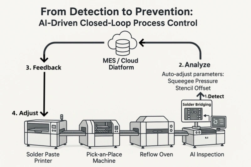
Solder paste printing is the initial stage of the SMT process, and its quality is critical to the final soldering result. Over 50% of solder joint defects can be attributed to improper solder paste printing. An AI system, combined with 3D imaging technology, measures and analyzes the solder paste's surface, height, volume, and shape. The AI model can accurately identify printing defects, providing a robust solution for PCBA solder paste inspection. It identifies issues such as solder paste offset, insufficient or excessive paste, bridging, and tailing. By performing real-time data analysis, the AI system can predict printing quality deviations and provide early warnings, enabling closed-loop control of the upstream process.
3.2 Post-Component Placement and Reflow Inspection
After component placement and reflow soldering, the AI system continues to perform a comprehensive inspection of components and solder joints:
- Component Defect Detection: It identifies missing components, wrong parts, polarity errors, and component skewing.
- Solder Joint Defect Analysis: Solder joints are complex three-dimensional objects with subtle morphological differences. By learning from a large number of images of good and bad solder joints, deep learning can identify and classify complex solder joint inspection defects, such as cold joints, cracking, and solder voids.
- Technical Extension: For solder joints under BGA packages, a 3D deep learning model combined with X-ray tomography can achieve a defect recognition rate of 99.2%.
3.3 Expanding Capabilities: AI Inspection for Specialized Processes and Components
Beyond standard SMD components, AI visual inspection proves to be exceptionally powerful in handling specialized manufacturing processes and complex components that traditionally challenge rule-based AOI systems.
Through-Hole Technology (THT) Component Inspection:
While SMT dominates modern PCB assembly, THT components remain critical in many applications for their mechanical strength and reliability. AI systems are trained to inspect the quality of through-hole solder joints. Using high-resolution side-view or angled cameras, the AI can assess:
- Solder Fillets: Evaluating the concavity/convexity and fullness of the solder around the pin and barrel to identify insufficient solder or voids.
- Solder Flags: Detecting excess solder that has wicked up the component lead, potentially indicating a process issue.
- Pin Presence and Bending: Verifying that all pins of a connector or header are correctly inserted and not bent prior to or during soldering.
Complex Connector and Multi-pin Component Inspection:
Components like board-to-board connectors, sockets, and headers present a high-risk area due to their pin count and density. AI vision excels here by performing precise, multi-attribute checks:
- Coplanarity Detection: For multi-pin connectors, even a slight warp or bend in the housing can prevent all pins from making a reliable connection. AI algorithms can accurately measure the height and alignment of every pin to ensure they lie on the same plane.
- Pin Damage and Contamination: Identifying bent, missing, or corroded pins with high accuracy, even when partially obscured by the connector housing.
- Polarity and Orientation Verification: Ensuring that asymmetrical connectors (e.g., USB, HDMI ports) are placed with the correct orientation and are not reversed.
The adaptability of deep learning models allows them to be trained on the unique morphological features of these diverse components and solder joints, providing a unified and robust inspection solution that eliminates the need for multiple specialized rule-based algorithms. This significantly reduces programming time for new PCB designs and ensures consistent quality across the entire assembly.
4. AI vs. AOI: A Technical Comparison for PCB Inspection
The following table compares the core differences between the two technologies:
|
Capability Dimension |
Traditional AOI |
AI Quality Inspection |
|
Inspection Principle |
Preset rule-based programming |
Deep learning + data training |
|
Defect Coverage |
Only rule-defined defects |
Can learn implicit features (e.g., micro-cracks) |
|
Dynamic Adaptability |
Requires manual parameter tuning |
Can be optimized via online incremental learning |
|
False Positive Rate |
>30% |
<8% (average measured) |
|
Complex Scene Handling |
Prone to interference from lighting/textures |
High robustness |
4.1 Case Study on Defect Handling Capabilities
Traditional AOI systems rely on pre-set rules (e.g., copper trace width tolerance), but when processing complex copper traces or light reflections, they can easily misjudge a harmless feature as a defect. For example, in High-Density Interconnect (HDI) board inspection, traditional AOI has a false positive rate of 60% because it cannot distinguish between laser marking reflections and actual scratches.
An AI inspection system overcomes this challenge through autonomous learning:
- Handling complex visual information: It effectively distinguishes between genuine defects (such as micro-scratches and irregular solder voids) and process deviations.
- Detecting hidden defects: It can analyze X-ray images to detect internal defects (solder voids, misaligned inner traces).
- Quantitative improvement: The false positive rate is reduced from 40%-50% to less than 10%, and the surface defect detection rate reaches 98%. This ability to significantly improve manufacturing defect analysis is a key advantage.
5. Implementation Challenges and Technical Development Trends
Despite the significant advantages of AI inspection, there are still challenges that require a collaborative approach.

5.1 Technical and Talent Barriers
AI inspection requires a deep integration of domain knowledge and AI technology. PCB engineers must understand AI mechanisms to guide model training, for example, by distinguishing between a true defect and a process variation.
5.2 Data Cost
Because of the high yield rate of PCBs, defect samples are rare. Solutions include few-shot learning and using GANs to synthesize defect data.
5.3 Customization Requirements
The highly customized nature of PCBs means that new product lines require new data collection and model retraining. This necessitates establishing a continuous iteration mechanism.
5.4 The Future of Smart Manufacturing
AI will be deeply integrated with the Industrial Internet of Things (IIoT) and Cyber-Physical Systems (CPS) to drive manufacturing quality control automation.
- Shifting from post-production sorting to defect prediction → closed-loop process feedback (e.g., early warnings of parameter deviations during the SPI stage).
- 3D deep learning models: Pushing breakthroughs in the detection accuracy of hidden solder joints like those found in BGA/CSP packages.
Conclusion
With the development of the Industrial Internet of Things (IIoT) and Cyber-Physical Systems (CPS), AI vision quality inspection will be deeply integrated with smart manufacturing, driving the intelligence and automation of production processes. In the future, AI will not only be for defect detection but will also enable defect prediction and closed-loop process feedback, improving production efficiency and product quality. As an important participant in the pcb manufacturing industry, NextPCB will continue to drive the development of AI vision inspection technology, providing customers with more efficient and accurate quality control solutions.
Through continuous technological innovation and practical application, NextPCB is committed to advancing the PCB manufacturing industry toward a more intelligent and automated future, providing global customers with high-quality and reliable PCB products and services.