
 NextPCB Capabilities
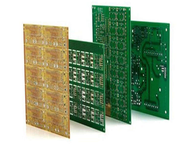
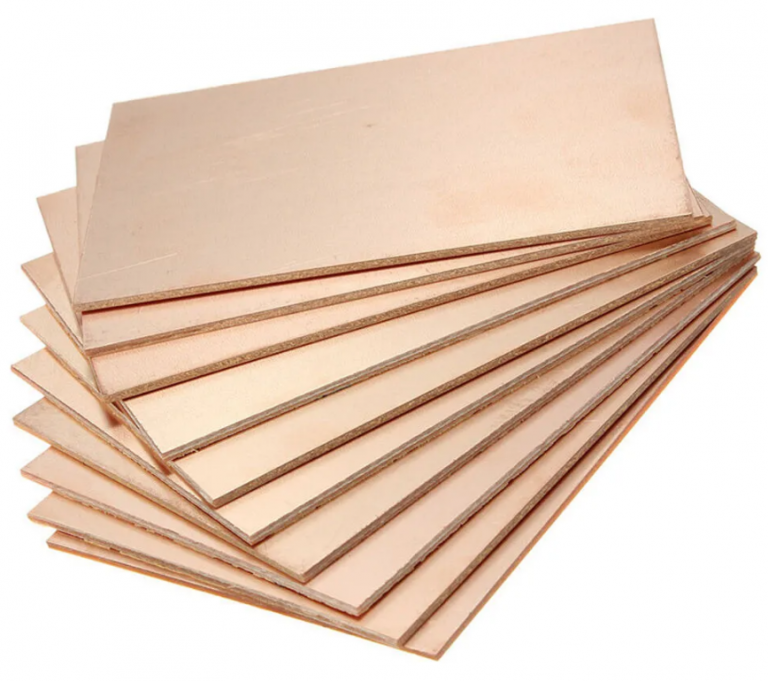
Printed Circuit Boards
NextPCB Capabilities
Printed Circuit Boards
 PCB Assembly
 Layer Buildup
 SMD-Stencils
 PCB Design-Aid & Layout
 Mechanics
 Quality
 Drills & Throughplating
 Factory & Certificate
 PCB Assembly Factory Show
Certificate
PCB Assembly Factory Show
Certificate
Support Team
Feedback:
support@nextpcb.com


In the world of Printed Circuit Boards (PCBs), 1oz Copper thickness plays a crucial role in determining the performance and functionality of the board.
Copper is often used in PCBs because it conducts electricity and heats well. But the thickness of the copper can change depending on the project. This article will look at the standard 1oz copper thickness in PCBs and why it matters for manufacturing.
In this article,
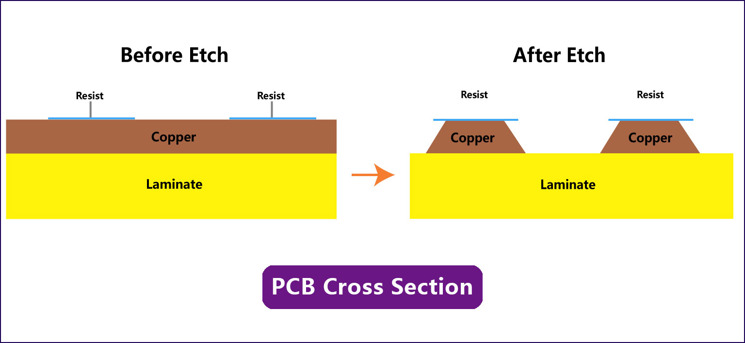
The standard copper thickness in PCB (Printed Circuit Board) refers to the thickness of the copper layer that is used to create the electrical connections on the board. Copper is an excellent conductor of electricity, and it is the primary material used for this purpose. '1oz copper thickness' means the thickness of copper on a PCB.
The measurement is carried out in ounces per square foot. When we say '1oz copper thickness', it means there is one ounce of copper on every square foot of the board.
It is important to note that the copper thickness of a PCB can affect the overall performance and reliability of the board. Proper selection and specification of the copper thickness should take into account the intended use of the PCB and any specific requirements or constraints that may be present.
Here is a brief point-to-point explanation of how the thickness of copper in PCBs can be varied for different applications:
In some cases, a thicker copper weight may be required for a PCB design. For example, if the board is designed to handle high current loads, a thicker copper weight may be necessary to prevent overheating and damage. Thicker copper can also help to reduce resistance and improve conductivity in certain applications. However, thicker copper also comes with a higher cost and may require more specialized manufacturing processes.
Thinner copper may be used for designs that require smaller traces and spaces or for applications where weight is a concern. Thinner copper can also be used to reduce the overall cost of the board, as it requires less copper and can be etched more quickly. However, thinner copper may not be suitable for applications that require high current or conductivity.
Trace Width:
The trace width is the width of the 1oz copper thickness conductor in a PCB.
The more 1oz copper thickness required to cover the trace, the thicker the copper layer will be, making the trace wider. Conversely, narrow traces require less copper, resulting in a thinner copper layer. For example, a 5-mil trace requires less copper than a 20-mil trace, resulting in a thinner copper layer for the former.
Current Carrying Capacity:
The amount of current a trace can carry depends on the trace's width and thickness. Thicker copper layers can carry more current without overheating or damaging the trace. As a result, high-current applications require thicker copper layers to avoid damage to the PCB.
Thermal Management:
Copper is good at carrying heat, and thicker layers help cool things down. When the circuit board requires high power, thicker copper is necessary to prevent overheating and breakdown.
Manufacturing Process:
The amount of copper on a PCB depends on how it's made. A process called electroplating adds copper to the surface using a tank. How long it's plated, how much solution is used, and how strong the current is, determine the thickness of the copper. Changing these things can create PCBs with different amounts of copper.
Cost:
Copper costs a lot, and using more of it makes things more expensive. So, when making a PCB, the amount of copper used depends on how well it needs to perform and how much it costs to make.
Current Requirements
The amount of current that a circuit needs to handle is one of the most critical factors in determining copper thickness. As the current increases, the resistance of the copper pathways also increases, leading to power losses and heat dissipation. Choosing thicker copper layers is preferable for high-power applications since they can sustain more current without overheating.
Thermal Management
Cooling is important in PCB design, especially for high-power devices. Bigger copper layers can help by giving more space for electrical paths and cooling. But, they can also make the PCB heavier and more expensive.
Signal Integrity
Copper thickness can mess up the circuit. It might bounce signals around and make them worse. If you want fast circuits, go for thinner copper to keep everything clear and precise.
Cost
1oz copper thickness can significantly impact the cost of the PCB. Thicker copper layers require more copper, which can increase the cost of the PCB. However, thinner copper layers may require more advanced manufacturing techniques and can also increase the cost of the PCB.
Current carrying capacity
The current-carrying capacity of a PCB is directly proportional to the 1oz copper thickness. If you expect the PCB to carry a higher current, you need to use a thicker copper layer. A 1oz copper thickness is ideal for a current range of 1-2A. If you want to increase the requirements, then it is advisable to opt for thicker copper layers. For instance, a 2oz copper thickness is ideal for a current range of 2-4A.
In the next part, we'll contrast regular 1oz copper thicknesses with other frequently utilized copper thicknesses in the industry. We'll check out how they affect the performance and reliability of the PCB.
2oz Copper in PCB:
2oz copper in PCB means that the copper layer on the board has a thickness of 2 oz/ft², which is equal to 2.8 mils or 0.07112mm. It is twice as thick as the standard 1oz copper and provides a lower resistance path for high-current circuits.
Power supply circuits, motor control circuits, and other high-current carrying capacity applications commonly utilize them. However, it comes at a higher cost, and the increased thickness may affect the board's flexibility and manufacturability.
3oz Copper in PCB:
3oz copper in PCB means that the copper layer on the board has a thickness of 3 oz/ft², which is equal to 4.2 mils or 0.10668mm. It is three times as thick as the standard 1oz copper and provides an even lower resistance path for high-current circuits.
This actively powers devices that require high levels of energy, such as robust LED lights, RF amplifiers, and circuits that actively handle substantial electrical loads. But it costs more than regular copper and might need special ways of making it.
0.5oz Copper in PCB:
0.5oz copper on a PCB means the copper layer is 0.5 ounces per square foot. That's about 0.7 mils thick or 0.01778mm. It's thinner than the usual 1oz copper and works well for low-power digital and RF circuits that don't need to carry as much current.
In conclusion, the thickness of standard 1oz copper in PCB is 1.4 mils or 35 microns. To ensure that the copper tracks on the PCB carry the required amount of current without overheating or getting damaged, it is essential to maintain a certain thickness.
In summary, the thickness of standard 1oz copper in PCB is a critical factor that affects the overall performance and functionality of the PCB. By understanding the importance of copper thickness and taking the necessary steps to ensure its accuracy, engineers can create robust and reliable PCBs that meet the needs of a wide range of applications.
Still, need help? Contact Us: support@nextpcb.com
Need a PCB or PCBA quote? Quote now


 Surface

