
 Surface


Lolly Zheng- Sales Account Manager at NextPCB.com

 NextPCB Capabilities
Printed Circuit Boards
NextPCB Capabilities
Printed Circuit Boards
 PCB Assembly
 Layer Buildup
 SMD-Stencils
 PCB Design-Aid & Layout
 Mechanics
 Quality
 Drills & Throughplating
 Factory & Certificate
 PCB Assembly Factory Show
Certificate
PCB Assembly Factory Show
Certificate
Support Team
Feedback:
support@nextpcb.com


Table of Contents
Vias are indispensable elements in the design of multilayer Printed Circuit Boards (PCBs), serving the essential function of establishing electrical connections between different conductive layers. They form the fundamental structure for transmitting high-speed signals, carrying high-current power and ground connections, and enabling efficient thermal management. In modern high-density and high-frequency electronic products, vias are the cornerstone for achieving complex layouts and functional integrity.
However, vias are not always benign. In high-speed applications, the impedance discontinuity they introduce presents one of the greatest challenges for Signal Integrity (SI) engineers. While vias provide necessary interconnect channels, they also bring parasitic effects, potential manufacturing defects, and increased cost. Therefore, the core engineering questions are: "When is the use of vias necessary in PCB design?" and "How can vias be reasonably used and optimized in high-frequency, high-density, and high-power scenarios?"
This article aims to provide a decision-making framework based on performance, cost, and Design for Manufacturing (DFM), combined with specific quantitative analysis and design practices. This will help engineers accurately determine when and how to select and optimize vias to ensure the best balance of electrical performance, reliability, and cost-effectiveness.
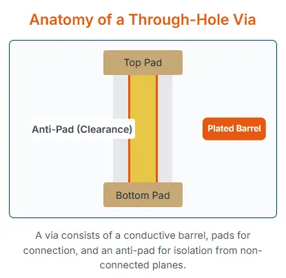
Vias are plated holes in the PCB that connect traces, pads, or plane conductors on different layers. Their presence significantly enhances the routing freedom of multilayer PCBs, allowing designers to meet complex layout requirements. A via typically consists of a plated copper barrel, a pad used for connecting traces, and an Anti-pad (clearance area) on reference planes, the latter used to prevent the plating from causing a short circuit to the plane layer. Vias are essential for accessing signal layers, plane layers, and providing connections to components.
The selection of via type is a critical decision that must be made early in the design process, as different types directly impact routing density, signal integrity, manufacturing complexity, and cost.
> Recommend reading: What is a Via in PCB Design and Every Via Type
Which PCB via types can HQ NextPCB produce?
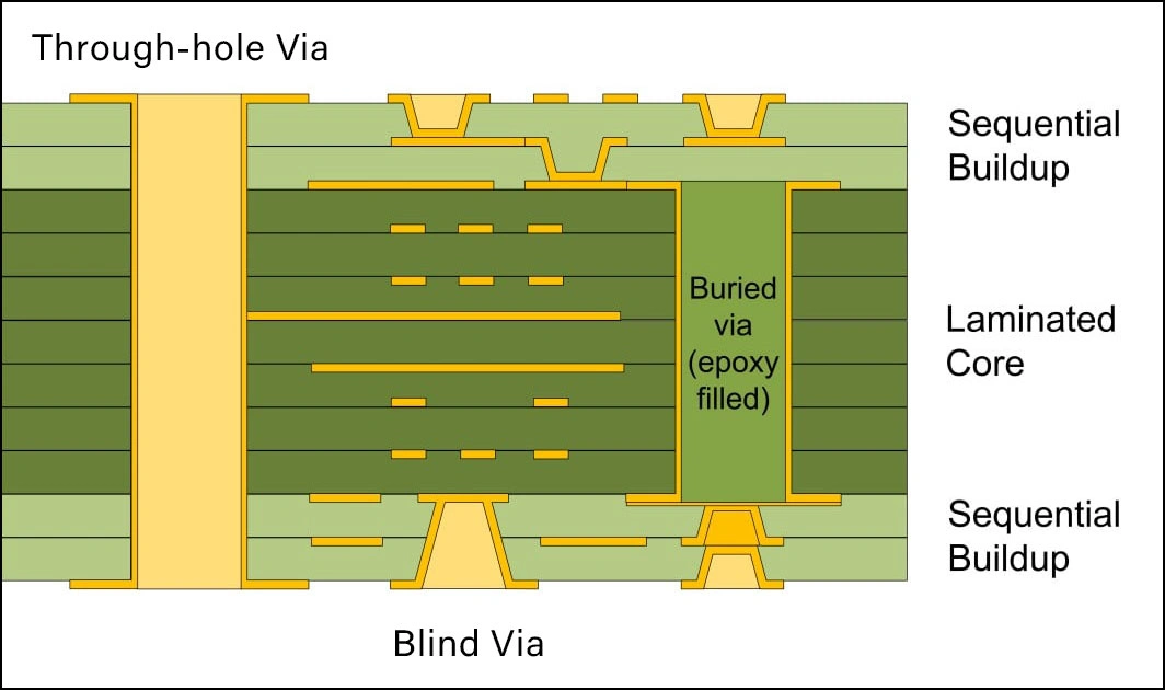
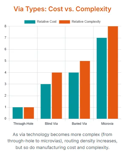
These are the most common type, passing through the entire board thickness and connecting all conductive layers. Their manufacturing process is simple, cost is lowest, and they offer high mechanical strength, often used for connectors or power components requiring structural support. The main drawback is the risk of Via Stub issues in high-speed designs and the consumption of routing space on all layers.
Blind vias start on an outer layer and terminate at an inner layer, but do not penetrate the entire board. They effectively save inner-layer routing space and increase routing density. For high-speed signals, blind vias minimize stub length, making them a standard feature in High-Density Interconnect (HDI) boards. Although blind vias save space and minimize stub length, over-reliance on them in high-speed applications can increase cost and manufacturing difficulty, requiring a balance between routing density and manufacturing feasibility.
Buried vias connect only two or more internal layers and are invisible from the outer surfaces. They save outer-layer routing space and are particularly suitable for isolated high-speed or complex signal connections internally. Manufacturing buried vias requires sequential drilling, plating, and multiple lamination cycles, increasing manufacturing validation complexity.
These are extremely small-diameter vias (typically ≤ 150 µm), usually created by laser drilling. Microvias are key to fanning out fine-pitch BGAs and implementing HDI structures, offering extremely high routing density. They are also critically important in high-frequency design because they reduce parasitic effects in the signal transmission path.
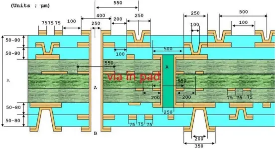
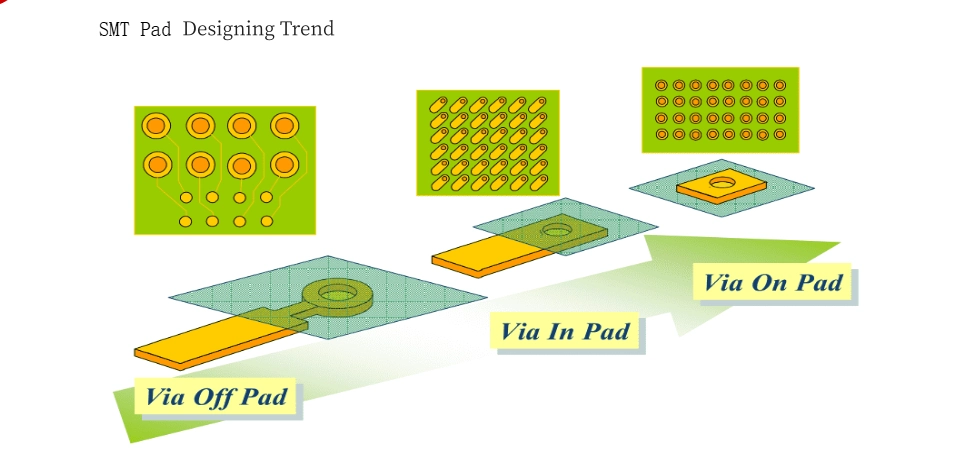
This technique places the via directly within the component's surface-mount pad. It minimizes the footprint, making it the primary method for fine-pitch BGA fanout. To ensure reliable SMT assembly, these vias must be filled and capped (VIPPO) to guarantee the pad surface is planar.
The choice of via type reflects the engineering trade-off between design density and cost. Manufacturing complexity and cost increase sequentially as via types upgrade from through-hole to blind, buried, and microvias. This increase is primarily due to the increased refinement in the manufacturing process; for instance, blind and buried vias require extra sequential drilling, plating, and multiple lamination steps, while microvias rely on high-precision laser drilling technology.
Although these complex via structures are more expensive, they significantly mitigate the negative impact on signal integrity in high-frequency applications by minimizing stub length and parasitic effects.
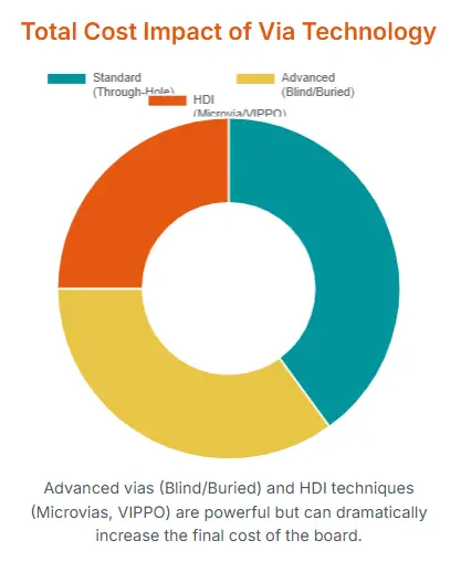
For modern engineering decisions, the pursuit of miniaturization and high integration leads to extremely dense BGA packages. In such scenarios, standard through-hole vias occupy too much routing space. Using blind/buried vias or microvias to solve high-density fanout issues is often no longer an optional optimization but a mandatory requirement for high-density designs. Therefore, engineers must ensure, through DFM checks, that the chosen complex via structure (e.g., blind/buried vias or microvias) falls within the manufacturer's capabilities, balancing design density and cost to enhance design manufacturability.
> Visit PCB Capabilities - NextPCB
In multilayer board design, signals inevitably need to jump from one layer to another to complete all network connections. This is the most fundamental and primary driver for using vias.
Designers should minimize unnecessary jumps by optimizing the layer stackup, placing coherent signal groups (e.g., differential pairs) on adjacent signal layers, and ensuring they are referenced to a solid plane. Even when a jump is mandatory, the "electrically shortest" principle should be maintained. This means the signal should transition via the shortest path possible to minimize parasitic effects like via inductance and capacitance, preventing unnecessary signal reflection and attenuation, thus maintaining signal integrity. To mitigate reflections and delays caused by transitions, it is recommended to route the same signal group (e.g., differential pairs) on adjacent layers, ensuring the signal transitions over the shortest path.
> Design rules: 15 Rules to Design the PCB Stackup
Vias are necessary for connecting power rails and ground planes (e.g., near decoupling capacitors) to provide a low-inductance, low-resistance path. In Power Integrity (PI) design, the current-carrying capacity of vias is a critical parameter.
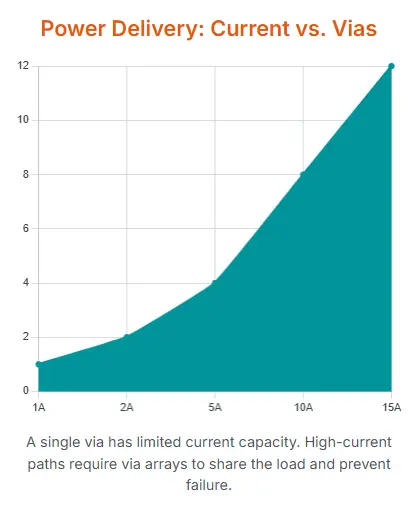
Overloading can cause via temperature rise, which may lead to delamination or circuit failure. Therefore, for high-current applications, the required number of vias must be determined through quantitative analysis. For instance, a standard 0.3 mm (12 mil) via with 1 oz copper plating can typically carry about 1.5 A of current within safe temperature limits.
More accurate current capacity can be approximated using the equivalent trace width method based on IPC standards (e.g., equivalent trace width can be approximated as diameter × π × 0.6).
For power rails with high current demands, a via array must be used to distribute the current, ensuring the temperature rise of each via remains within a safe range to prevent localized overheating that could lead to PCB delamination or circuit failure. Engineers can determine the minimum number of vias required for a safe and reliable connection using quantitative analysis or estimation (such as based on equivalent trace width).
When establishing reliable connections between power and ground planes, designers should use calculation tools (such as the equivalent trace width method in IPC standards) to precisely calculate the required number of vias, ensuring each can effectively carry the current and maintain temperature rise within safe limits. The decision on the number of vias in power design is not based on "Can it connect?" but on "Can it reliably carry the current and dissipate heat to meet product lifespan requirements?"—an upfront investment in thermal management and reliability. By dispersing current and heat flow, via arrays significantly reduce localized temperature rise, thereby extending component life and increasing PCB reliability according to the Arrhenius equation.
As BGA package pitches continue to shrink (e.g., < 1 mm), traditional dog-bone fanout is often no longer feasible. In this high-density routing scenario, Via-in-Pad (VIP) combined with filling and capping (VIPPO) becomes a mandatory choice to solve routing density bottlenecks. VIPPO maximizes the routing space around the pad, making it a critical choice for managing dense BGA area routing.
In high-power or thermally sensitive designs, Thermal Vias are mandatory structures used to conduct heat away from the component base (e.g., the thermal pad of QFNs or power MOSFETs) to internal ground planes or external heat sinks.
Heat dissipation efficiency is closely related to the design parameters of the thermal via array. Recommended hole diameters are between 0.2 mm and 0.4 mm (8 mil to 16 mil). A critical DFM consideration is the pitch (via-to-via distance): To prevent solder wicking during reflow soldering, which can compromise SMT reliability, the via pitch should be maintained between 1.0 mm and 1.2 mm (40 mil to 48 mil). Furthermore, thermal vias must connect to a solid copper plane to act as an efficient heat sink; thermal relief patterns should be avoided as they increase thermal resistance by limiting copper contact. Thermal via design is the intersection of electrical engineering, thermal engineering, and manufacturing engineering, where precise pitch control aims to balance high-performance heat transfer with high-yield SMT assembly.
Overusing vias can lead to potential negative effects, primarily manifesting in the following areas:
Designers should avoid using vias in non-essential cases through the following strategies:
> Recommend reading: Best 6-Layer PCB Stackups for Signal Integrity & Impedance Control
The routing density of fine-pitch BGAs forces designers to adopt HDI stackup structures. In BGA fanout, the use of Via-in-Pad (VIPPO) combined with microvias enables extreme routing density. For example, through a via-in-pad method, the space available for routing can be maximized. For complex HDI structures, such as backdrilling and blind/buried vias, NextPCB offers specialized DFM consulting services and precise manufacturing tolerance control to ensure high-yield fanout in BGA regions.
Upload File & Get Specialized DFM Consulting Services
In extremely high-speed design, a via must be treated as a small, lossy transmission line component, requiring precise design to ensure impedance continuity.
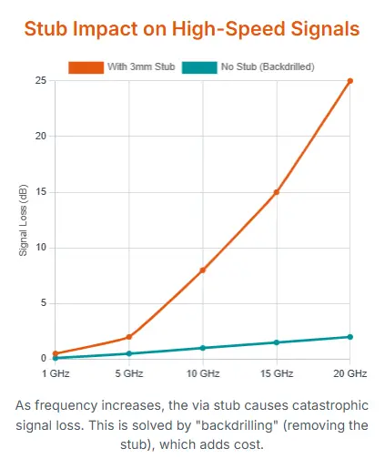
When a signal uses a through-hole via to connect to an internal layer, the unused portion of the via (the stub) can cause severe signal reflection, mode conversion, and insertion loss at high frequencies. At frequencies above 2 GHz, even a via stub as short as 0.5 mm can cause noticeable issues.
For high-speed signals (bandwidth above 1 GHz), Backdrilling is the most effective method for eliminating stubs. Backdrilling through physical removal of the residual barrel allows the stub length to be controlled to less than 10 mils (0.254 mm), which significantly restores impedance continuity. Backdrilling technology effectively removes the via stub, minimizing the via's length to reduce signal reflection and enhance signal integrity, making it an indispensable optimization technique, especially in high-frequency design. However, implementation faces challenges related to drilling precision, cost, and additional manufacturing time.
For certain applications, backdrilling may require specialized equipment or processes, so feasibility and cost-effectiveness should be considered during the design phase. While backdrilling increases cost and manufacturing time, it is essential for applications supporting data rates of 25 Gbps or higher.
A grounded via (stitching via) must be placed near the high-speed signal via to "stitch" the signal return current to the reference plane. This minimizes electromagnetic field leakage, reduces loop inductance, and suppresses EMI. In extremely high-frequency designs, maintaining signal integrity hinges on precise geometry design (hole diameter, anti-pad) and backdrilling to match the via impedance to the transmission line's characteristic impedance as closely as possible.
The via's Aspect Ratio (depth-to-diameter ratio) is a critical indicator of the difficulty of manufacturing the copper plating. A high aspect ratio can lead to uneven plating, reducing reliability. Blind and buried via manufacturing is particularly complex, relying on multi-step lamination and plating. Blind and microvias require high-precision laser drilling or sequential plating processes, and an unreasonable aspect ratio can lead to uneven plating quality, compromising connection reliability. Therefore, the design must conform to the manufacturer's specifications. Designers must ensure the design complies with the manufacturer's minimum hole diameter, layer-to-layer connection methods, and other specifications.
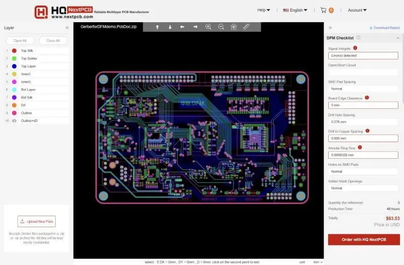
With one click, HQDFM will export a report detailing each issue and give suggestions on how to resolve them.
Try it for free (no sign-up required).
Annular Ring and Tolerance: Drilling position tolerance dictates the minimum Annular Ring size that must be reserved on the pad to prevent connection breakage due to drill misalignment. IPC Class 3 designs require a larger annular ring size (e.g., 5 mil (0.127 mm)).
VIPPO Filling: Via-in-Pad (VIP) must be filled and planarized (VIPPO); otherwise, solder will drain into the hole during reflow, compromising component soldering reliability. For VIPPO technology, ensure that the manufacturer's DFM checking service can verify the accurate placement of the via in the pad and guarantee the quality of the filling and capping plating to prevent solder wicking and maintain soldering quality during reflow.
Manufacturer Collaboration: Engineers should work closely with the PCB manufacturer from the design stage, utilizing DFM checking services provided by companies like NextPCB, to pre-verify the stackup structure, via aspect ratios, and blind/buried via configurations, ensuring complex designs can be smoothly and economically manufactured at scale.
Vias are an essential element of multilayer PCBs, but their use must be a well-considered engineering decision. The rational use of vias is key to ensuring signal integrity, efficient thermal management, cost-effectiveness, and manufacturability.
The precise selection and use of vias are critical for achieving high-performance, high-reliability PCB designs. Designers must accurately choose the appropriate via type based on signal integrity, current capacity, and thermal management considerations, ensuring the design aligns with the manufacturer's capabilities to control costs while guaranteeing performance.
In design, vias should be treated as transmission line discontinuities requiring precise optimization, selecting the most appropriate type and array based on signal speed and current load. In low-speed designs, standard through-hole vias are the most cost-effective choice; conversely, in high-speed, high-power applications, techniques such as blind vias, backdrilling, stitching vias, and thermal via arrays must be employed to maintain system reliability.
Optimizing the design to enhance overall system performance while collaborating with professional manufacturers to mitigate manufacturing risks and costs is the road to success in modern electronic design.

Still, need help? Contact Us: support@nextpcb.com
Need a PCB or PCBA quote? Quote now

