
 NextPCB Capabilities
Printed Circuit Boards
NextPCB Capabilities
Printed Circuit Boards
 PCB Assembly
 Layer Buildup
 SMD-Stencils
 PCB Design-Aid & Layout
 Mechanics
 Quality
 Drills & Throughplating
 Factory & Certificate
 PCB Assembly Factory Show
Certificate
PCB Assembly Factory Show
Certificate

Support Team
Feedback:
support@nextpcb.com


MOSFETs, or metal oxide semiconductor field effect transistors, are one of the most versatile and powerful electronic components available. They can be used in a wide variety of applications, from switching power supplies to amplifiers. However, like any electronic component, MOSFETs can fail. If you suspect that a MOSFET in your circuit is bad, it is important to be able to test it quickly and easily.
This article will provide you with a comprehensive guide to testing MOSFETs. We will cover the following topics:
A metal–oxide–semiconductor field-effect transistor (MOSFET, MOS-FET, or MOSFET) is a type of field-effect transistor (FET), most commonly fabricated by the controlled oxidation of silicon. It has an insulated gate, the voltage of which determines the conductivity of the device. This ability to change conductivity with the amount of applied voltage can be used for amplifying or switching electronic signals. A metal-insulator-semiconductor field-effect transistor (MISFET) is a term almost synonymous with MOSFET. Another synonym is IGFET for the insulated-gate field-effect transistor. If you want a deeper look at the internal physics behind this behavior, see our guide on How Does a MOSFET Work?
MOSFETs are available in both n-channel and p-channel configurations. In an n-channel MOSFET, the majority of carriers are electrons, while in a p-channel MOSFET, they are holes. MOSFETs also have different voltage ratings, current ratings, and on-resistance ratings, which make them suitable for various applications. If you are evaluating which transistor technology best fits your design, our article on the difference between MOSFET and BJT and how to choose is a useful starting point.
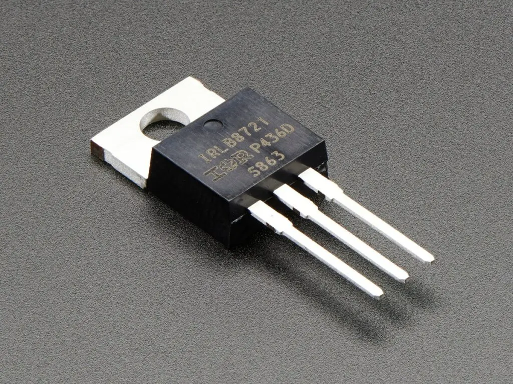
These are commonly applicable for switching applications, as they can be rapidly turned on and off. MOSFETs are widely used in many different applications due to their ability to amplify signals with very little distortion and handle high voltages and currents without a great deal of power loss. To ensure the proper functioning of the circuit, it is essential to test these components. This is possible to achieve through in-circuit or out-of-circuit testing, as well as the use of advanced test equipment.
MOSFETs necessitate the utilization of special instruments and tools to examine them. A few examples of frequently used equipment and apparatus include:
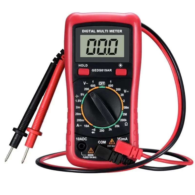
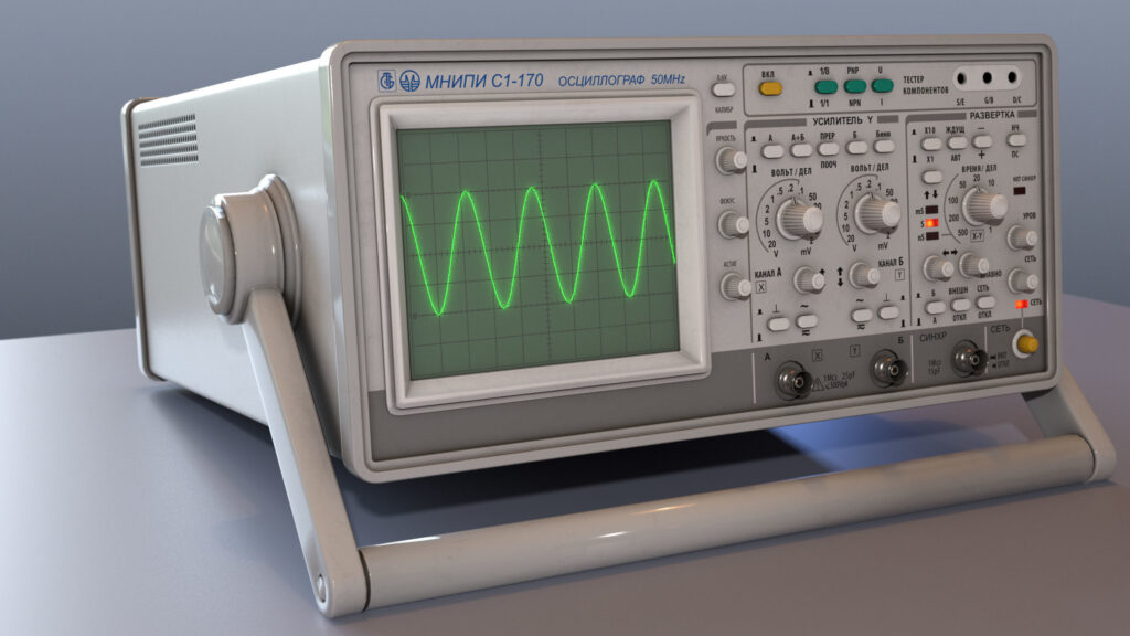
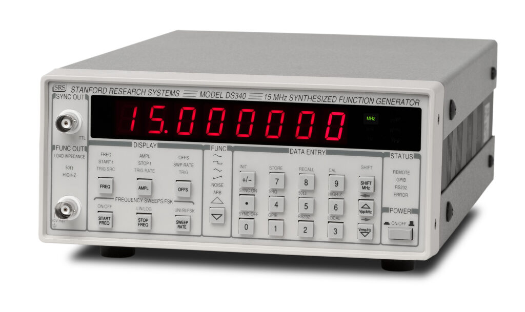

For reliable and precise results, it is critical to use the right equipment and tools when assessing MOSFETs.
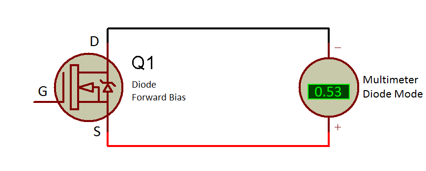
This easy-to-follow guide will lead you through the process:
Testing a MOSFET with a digital multimeter (DMM) is the most practical method for field engineers and hobbyists alike. No specialized equipment is required — a standard multimeter in diode-test or resistance mode is sufficient to quickly determine whether a MOSFET is functional or faulty.
Use the table below to quickly interpret your DMM readings when performing a MOSFET test with a multimeter:
| Test | Good MOSFET Reading | Bad MOSFET Reading | Likely Fault |
|---|---|---|---|
| Drain–Source (off state, diode mode) | 0.4 V – 0.7 V (one direction), OL (reverse) | 0 V or OL in both directions | Shorted or open D-S |
| Gate–Source resistance | OL (very high, >1 MΩ) | Low resistance (<1 kΩ) | Gate oxide failure / leakage |
| Drain–Source (gate charged, on state) | Very low resistance / near 0 V drop | High resistance or OL | Open channel / failed junction |
| Drain–Source (gate discharged, off state) | Returns to OL (open) | Remains at low resistance | Shorted drain-source |
Tip: Always perform the MOSFET diode test first. If you see 0 Ω between Drain and Source regardless of gate state, the MOSFET is shorted and must be replaced. If you see OL in all conditions including the on state, the channel has failed open.
Knowing how to identify a damaged MOSFET quickly can save hours of troubleshooting. A bad MOSFET typically presents through a combination of visual symptoms and abnormal electrical readings. Here is what to look for:
| Characteristic | Good MOSFET | Bad MOSFET |
|---|---|---|
| Gate-Source resistance | Very high (>1 MΩ) | Low (<1 kΩ) — gate oxide damage |
| Drain-Source (gate off) | Open circuit (OL on DMM) | Low resistance — shorted |
| Drain-Source (gate on) | Low resistance / conducting | High resistance / open — broken channel |
| Body diode forward drop | 0.4 V – 0.7 V | 0 V (shorted) or OL (open) |
| Visual appearance | Clean, no marks | Burn marks, discoloration, cracks |
| Switching behavior | On/off with gate voltage | Stuck on, stuck off, or erratic |
The test procedure varies depending on whether you are working with an N-channel or P-channel MOSFET. Understanding the polarity difference is essential to getting correct multimeter readings. For a broader comparison of how these two types differ in design and application, see our guide on PMOS vs NMOS: Focus on Two Main Forms of MOSFET.
N-channel MOSFETs are the most common type and are turned on by applying a positive voltage to the Gate relative to the Source.
P-channel MOSFETs operate with reversed polarity — they turn on when the Gate voltage is lower than the Source voltage (negative Vgs).
When you need to test a MOSFET without removing it from the board, keep the following in mind:
Depending on the specific application, people can test MOSFETs in various ways. When constrained by circuit board connection, an in-circuit test is necessary to detect any potential faults that may exist – providing engineers with valuable insight into device performance. Engineers often prefer this method when the fault relates to the circuit itself or when the MOSFET is not easy to remove.
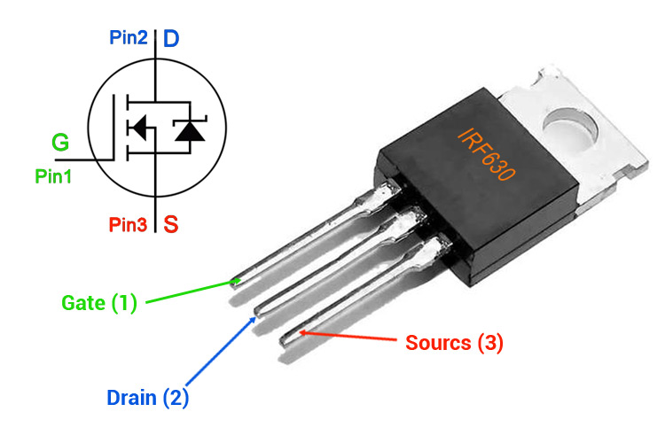
People can do in-circuit testing using a multimeter or MOSFET tester and can include tests such as measuring the threshold voltage, drain-source resistance, and gate leakage current.
If other components are affecting the measurements, in-circuit testing may not provide accurate results.
By eliminating the MOSFET from its circuit board and testing it independently, we can achieve more reliable results through out-of-circuit testing. Rephrased: Out-of-circuit testing allows for more reliable results because it eliminates the risk of other components connected to the MOSFET affecting measurements.
Out-of-circuit testing can be done using a MOSFET tester and can include tests such as measuring the threshold voltage, drain-source resistance, and gate leakage current. To ensure a reliable and safe operation, out-of-circuit testing should also involve visually examining the component for any indications of physical damage or overheating.
Ultimately, both in-circuit and out-of-circuit testing have their own distinct benefits as well as drawbacks. In-circuit testing is faster and more convenient but may not provide accurate results if there are other components affecting the measurements. Rephrased: Achieving more precise results through out-of-circuit testing involves the removal of the MOSFET from the circuit board, which is a time-consuming process that may require specialized tools. The choice of testing method depends on the specific application and the nature of the fault.
There are several common faults that can occur, including:
Identifying faults can be challenging, but by following proper testing procedures and taking appropriate precautions, faults can be identified and resolved.

When troubleshooting MOSFET circuits, it is important to follow a systematic approach to identify the cause of the fault. Here are some steps to follow when troubleshooting circuits:
Diagnosing and repairing MOSFET circuits can be an intimidating prospect, but with the right approach, it's possible.
Yes, it is possible to test a MOSFET without removing it from the PCB using a multimeter. However, parallel components on the board can interfere with measurements. If results are inconclusive, desolder one pin to isolate the device for a more accurate reading.
A bad MOSFET typically shows one or more of these signs: a shorted drain-source (low resistance in both directions), gate-source leakage (low G-S resistance), failure to switch on or off with gate voltage, burn marks or discoloration on the package, or abnormally high on-state resistance (Rds(on)).
Continuity in one direction between Drain and Source is normal — it is the body diode of the MOSFET. However, if you see very low resistance (near 0 Ω) in both directions regardless of gate state, the MOSFET has a shorted drain-source and is faulty.
Yes. A MOSFET can degrade partially — for example, showing higher-than-specified Rds(on), reduced gate threshold voltage, or increased gate leakage — before failing completely. Partial failures can be identified by comparing DMM readings to datasheet specifications.
The probe polarity is reversed. For an N-channel MOSFET, the body diode forward drop is measured with the red probe on Drain and black on Source. For a P-channel MOSFET, swap the probes: black on Drain and red on Source. The gate trigger polarity is also reversed — P-channel devices turn on with a negative Vgs.
A standard digital multimeter (DMM) with a diode-test mode is sufficient for basic pass/fail testing. For more detailed characterization (threshold voltage, Rds(on), transconductance), a dedicated MOSFET tester or a curve tracer provides far more accurate results. For production-level PCBA testing, functional test fixtures and automated test equipment (ATE) are recommended.
Manual multimeter testing is invaluable for bench-level diagnostics, but when your design moves toward production, individual component checks are no longer enough. A MOSFET that passes a bench test can still fail in-circuit due to layout parasitics, thermal crowding, gate drive signal integrity issues, or subtle component interactions that only appear under real operating conditions.
This is where professional PCBA testing and engineering support make a critical difference.
If you are still at the prototype stage — debugging switching behavior, hunting for a shorted MOSFET that only fails under load, or unsure whether the problem is the component or the PCB layout — NextPCB's Rev0 PCBA Service is designed exactly for this situation.
Rev0 is NextPCB's rapid prototyping and engineering support service for early-stage hardware teams. It combines fast-turn PCB fabrication and PCBA with hands-on engineering review, so that issues like gate drive problems, thermal failures, and MOSFET switching anomalies are caught and diagnosed before they become costly production defects.
Whether you are designing a power supply, a motor driver, or any circuit where MOSFETs are critical, getting the prototype right the first time saves significant time and cost. Learn more about NextPCB Rev0 PCBA →
Because MOSFETs have an insulated gate, they act like tiny capacitors. If you do not short the Gate and Source pins before testing, the MOSFET can retain a charge and stay in the "on" state. This will result in false multimeter readings, making a perfectly healthy MOSFET appear as though it has a shorted drain-source path.
Testing an SMD MOSFET utilizes the exact same electrical principles as testing a standard through-hole component. The primary challenge is the physical size. You will need fine-tipped multimeter probes or specialized testing tweezers. Always refer to the datasheet first, as the pinout configurations (Gate, Drain, Source) on compact packages like SOT-23 or SO-8 look completely different from standard TO-220 packages.
Overheating can cause the MOSFET to fail and can be identified by a burnt smell, discoloration, or visible damage, or by measuring the temperature with a thermometer or thermal imaging camera[cite: 1]. If a MOSFET is overheating in the "on" state rather than functioning smoothly, the most common culprit is a lack of gate drive. An insufficient gate voltage can cause the MOSFET to not turn on fully, resulting in higher-than-expected drain-source resistance[cite: 1]. This excess resistance converts the current passing through the component directly into waste heat.
Yes, but it requires a slightly different approach and is generally less precise. Analog multimeters often output higher voltages on their high-resistance settings (like the Rx10k scale), which is usually enough to charge the gate and turn the MOSFET on. However, interpreting the needle swing is subjective compared to the clear forward-voltage readings provided by a digital multimeter (DMM) in diode-test mode. Therefore, a DMM is highly recommended for accurate diagnostics.
In conclusion, testing and troubleshooting MOSFETs require careful attention and adherence to proper procedures to ensure accurate results and avoid damage to the circuit or other components. By using the appropriate tools and equipment, following established testing procedures, and taking appropriate safety precautions, it is possible to identify and resolve faults efficiently.
When diagnosing and testing MOSFET circuits, it is essential to use effective procedures that consider the factors influencing performance. Careful consideration should be given to in-circuit versus out-of-circuit tests as well as common faults while consulting with corresponding datasheets for detailed specifications and guidelines. Recording measurements taken during setup helps engineers save time troubleshooting future issues while avoiding costly repairs of operational systems. By following best practices when conducting these tests, technicians can ensure reliable outputs from their circuitry projects!
Don't be intimidated by a technical issue, get expert help from an engineer or technician and skillfully resolve it. They can ensure that all testing and procedures are performed appropriately for optimal results. With careful attention and proper procedures, MOSFET testing and troubleshooting can be an effective way to maintain the reliability and performance of electronic circuits.
Still, need help? Contact Us: support@nextpcb.com
Need a PCB or PCBA quote? Quote now



 Surface

