
 Surface


Stacy Lu

 NextPCB Capabilities
Printed Circuit Boards
NextPCB Capabilities
Printed Circuit Boards
 PCB Assembly
 Layer Buildup
 SMD-Stencils
 PCB Design-Aid & Layout
 Mechanics
 Quality
 Drills & Throughplating
 Factory & Certificate
 PCB Assembly Factory Show
Certificate
PCB Assembly Factory Show
Certificate
Support Team
Feedback:
support@nextpcb.com


Table of Contents
The reliable operation of power electronics hinges on meticulous thermal management within the Printed Circuit Board (PCB) structure. When current flows through a conductor, the inherent resistance results in power dissipation, quantified by P = I2R. This energy loss manifests as heat, leading to a critical rise in the conductor’s temperature above ambient conditions, known as the Temperature Rise (TRISE).
The total operational temperature of the trace (TTEMP) is TTEMP = TRISE + TAMB.
PCB trace width calculation is a fundamental design process that determines the minimum required width of a copper conductor to safely carry a specified electric current. The primary goal is to ensure the conductor has the correct cross-sectional area to prevent overheating and potential damage to the board. This calculation utilizes standard industry formulas, such as those derived from IPC standards, to maintain the trace's temperature rise (TRISE) below a prescribed maximum value for a given maximum current. By factoring in parameters like ambient temperature and trace length, the calculation can also estimate critical performance metrics:
The authoritative standard for predicting trace temperature rise and determining the minimum trace width (W) is the IPC-2152 standard ("Standard for Determining Current Carrying Capacity in Printed Board Design"). This standard overcomes the limitations of the older, generalized IPC-2221 by incorporating critical variables such as board material, layer location, dielectric thermal conductivity, and the heat-sinking effect of adjacent copper planes, leading to more accurate and optimized trace width predictions.
While IPC standards provide necessary guidelines, complex, high-power designs require dedicated verification. Thermal Simulation and Verification tools (often employing Finite Element Analysis or Computational Fluid Dynamics) are essential for accurately predicting thermal performance in constrained operating environments, helping engineers account for temperature fluctuations and prevent overheating issues. These advanced simulations, which can model transient behavior to show how the PCB heats up or cools down over time, identify potential thermal problems such as hotspots, excessive current density in boreholes, and voltage loss before physical prototyping. By simulating the temperature increase triggered by power dissipation and high currents, designers can refine the layout or layer structure virtually, saving prototype costs and time. The objective of this early co-simulation is to ensure that performance targets, such as maximum operating temperatures (typically < 100°C), are met before the first board spin.
> Recommend reading: Choosing High-Speed PCB Stackups from 4 to 10 Layers
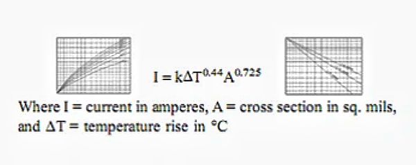
While superseded, the formula derived from the older IPC-2221 standard remains valuable for quick, conservative initial estimates. It quantifies the relationship between maximum current (IMAX) and the required cross-sectional area (A) using curve-fitting constants:
A[mils2] = (IMAX[Amps] / (k × (TRISE[°C])b))(1/c)
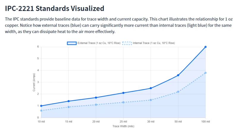
Where k, b, and c are non-physical constants. The constants explicitly differentiate between external and internal layers, with external traces benefitting from approximately twice the thermal efficiency (k = 0.048 for external layers vs. k = 0.024 for internal layers), justifying the design guideline that high-current traces should be routed on external layers whenever possible.
The practical implementation of IPC standards requires a systematic approach to calculating the physical dimensions of the conductor and modeling its electrical performance characteristics under operating conditions.
The design goal is to determine the minimum trace width (W) required to carry the maximum current (IMAX) without exceeding the allowed temperature rise (TRISE).
After establishing the required Area (A) in square mils (mils2) using the appropriate IPC formula, the trace width in mils (W[mils]) is calculated by dividing the area by the thickness of the copper foil:
W[mils] = A[mils2] / (Toz[oz] × 1.378[mils/oz])
Accurate modeling requires the ability to convert between the standard unit of copper thickness—ounces per square foot (oz)—and linear thickness units (mils or millimeters). 1 oz of copper, when uniformly compressed and flattened to cover 1 square foot of surface area, results in a linear thickness of 1.37 mils (or 0.0348 millimeters).
| Copper Weight (oz) | Thickness (mils) | Thickness (mm) | Thickness (μm) |
|---|---|---|---|
| 1.0 oz | 1.37 | 0.0348 | 34.80 |
| 1.5 oz | 2.06 | 0.0522 | 52.20 |
| 2.0 oz | 2.74 | 0.0696 | 69.60 |
| 3.0 oz | 4.11 | 0.1044 | 104.40 |
| 4.0 oz | 5.48 | 0.1392 | 139.20 |
The fundamental resistance (R) of a conductor is determined by the length (L), the cross-sectional area (A), and the material’s inherent resistivity (ρ):
Rtrace = ρ × (L / A)
A critical consideration is the positive Temperature Coefficient of Resistance (α) for copper, meaning its resistance increases as its temperature rises. At 20°C, copper resistivity (ρ) is approximately 1.72 × 10⁻⁸ Ω·m, and the TCR (α) is approximately 0.00393 / °C. For precise calculations, the resistivity must be adjusted for the expected operating temperature (T):
ρT = ρ20°C
Failing to account for this temperature effect can result in a significant underestimation of resistance and voltage drop; a temperature rise of 50°C can increase the trace resistance by approximately 18%.
> Recommend reading: The Resistor in Modern Electronics: Fundamentals, Advanced Applications, and Reliability
Once the temperature-adjusted resistance (R) is determined, the key performance metrics are calculated:
Achieving high-reliability in power designs demands practical strategies that extend beyond basic trace width calculation, focusing on strategic material use, layout optimization, and enhanced heat transfer mechanisms.
Because external layers offer approximately double the thermal efficiency of internal layers, high-current traces should reside on the top or bottom of the PCB. When internal routing is unavoidable, internal traces typically require 20 to 30 percent more width than external traces carrying the same current to achieve an equivalent temperature rise. For high-power applications (e.g., motor controls up to 50A), increasing the copper weight to 2 oz (70 µm) or more reduces resistivity and increases the conductor’s thermal mass.
> See more details at PCB Thermal Design Case Study: Copper Thickness for Uniform Heat Load
Thicker copper requires larger minimum feature sizes for high yield due to the etching process. The etching difficulty of heavy copper foil—especially 3 oz and 4 oz—reduces precision, leading to strict limits on minimum feature size and clearance. For high-density interconnect (HDI) designs that typically demand 2–3 mil clearance, this constraint often makes heavy copper infeasible.
> Learn Thicker Copper PCBs
| Copper Weight (oz) | Min. Recommended Space (mils) | Min. Recommended Trace Width (mils) |
|---|---|---|
| 1 oz | 3.5 mil (0.089 mm) | 3.5 mil (0.089 mm) |
| 2 oz | 8 mil (0.203 mm) | 8 mil (0.203 mm) |
| 3 oz | 10 mil (0.254 mm) | 10 mil (0.254 mm) |
| 4 oz | 14 mil (0.355 mm) | 14 mil (0.355 mm) |
This shows that increasing copper weight significantly penalizes routing density. For instance, moving from 1 oz copper to 4 oz copper requires a four-fold increase in the minimum recommended spacing (from 3.5 mil to 14 mil). This disproportionate increase in required separation significantly limits fine-pitch component placement and reduces the overall channel density of the PCB, forcing a crucial trade-off between thermal performance and board size/cost. Designers working with extreme heavy copper should consult specific manufacturer capabilities; for instance, NextPCB’s heavy copper options require minimum trace/spacing up to 5.5 mil/5.5 mil for 2 oz copper. For currents exceeding 100A (e.g., electric vehicles), the preferred solution is the incorporation of copper bus bars soldered directly onto the PCB.
Connecting high-current traces directly to expansive, solid copper planes significantly aids heat dissipation. IPC-2152 modeling shows that these solid connections can reduce the trace temperature by 20 to 50 percent compared to isolated traces.
Another technique to boost current capacity is the application of a solder overlay (filleting). This technique is primarily used in single-sided or pulse-load applications where a substantial increase in thermal mass is needed to safely handle high transient currents. By leaving traces bare (no solder mask), a thick layer of solder deposits during assembly, increasing the electrical cross-sectional area and the thermal mass. Testing has shown this technique can safely increase the current rating on 1 oz copper boards by approximately double, especially benefiting applications subject to high pulse loads.
While effective for current capacity, the thick solder layer creates significant long-term reliability and serviceability risks. The custom, heavy application of solder makes rework and repair (if needed) exceedingly difficult.
Furthermore, repeated or excessive exposure to high heat during rework can induce severe thermal stress in the PCB materials. This thermal stress can weaken existing solder joints, potentially cause layer delamination, and degrade electrical performance, consequently reducing the overall reliability and lifespan of the product. This trade-off must be carefully weighed: increased current capacity comes at the cost of diminished field repairability and thermal tolerance during maintenance.
High-current, heat-generating components should be centralized, away from board edges, to allow the entire PCB to participate in heat dissipation. Furthermore, tightly routing high-di/dt switching loops (e.g., in a half-bridge) minimizes parasitic loop inductance, which reduces switching losses and associated heat generation in the primary power path.
In multi-layer PCBs, the vertical conductivity managed by vias is often the weakest link in a high-current path. Vias must be treated as dedicated components whose current-carrying capacity must be rigorously calculated to prevent localized overheating.
> Recommend reading: Blind Vias and Buried Vias: What Is the Difference in PCB?
A via's resistance (R) is governed by the plated copper resistivity (ρ), the via length (L, or board thickness), and the cross-sectional area of the plating (A):
R = ρ × L / A
The via's resistance is calculated using this formula, where L is the board thickness (via length), ρ is the copper resistivity, and A is the cross-sectional area of the cylindrical copper plating. Input parameters for via current capacity calculators include plating thickness (typically 0.8–1.4 mils), via height, via diameter, and the acceptable temperature rise. These calculations yield critical outputs like resistance at ambient and high temperatures, voltage drop, and power loss, allowing designers to verify that the via's temperature rise remains within the safety limit.
Via stitching extends the conductor path across multiple layers, combining the cross-sectional area of several copper layers to handle elevated current. For thermal management, thermal via arrays are dense groupings placed underneath heat-generating components (like MOSFET exposed pads). These arrays act as highly efficient vertical thermal conduits, transferring heat to internal planes or a heatsink.
For high-current, multi-layer applications, the thermal advantage of multi-layer boards is only realized through effective vertical conduction via these arrays. The use of thermal vias (often smaller in diameter, such as 0.3mm or 12 mil plated) under heat sources is essential. These dense clusters efficiently transfer heat from the component's junction through the layers, achieving a significant reduction (e.g., 30%) in component operating temperature. Optimizing these arrays is critical for minimizing the temperature differential (ΔT) between layers beneath the heat source, often targeting ΔT < 5°C, to confirm maximized heat transfer into the bulk structure or external heat sinks.
High-current design often conflicts with robust manufacturing reliability, particularly concerning component connections.
Thermal reliefs are narrowed copper connections between a component pad and a large copper area (like a power plane). Their purpose is to increase localized thermal impedance to prevent large copper areas from acting as heat sinks, which can cause assembly defects like tombstoning or poor solder joint formation during reflow. However, thermal reliefs introduce a performance penalty by increasing both the thermal impedance (reducing the pad’s effectiveness as a heat sink) and the electrical impedance (adding small, parasitic resistance and inductance).
The choice must be strategic:
For high-reliability systems, relying solely on static calculations based on IPC charts is insufficient. The modern approach mandates the use of co-simulation, performing integrated electrical and thermal analysis early in the design cycle. This data-driven approach ensures performance targets, such as maximum operating temperatures (typically < 100°C) and safe current densities, are met before prototyping, avoiding costly board revisions.
Robust PCB design for high-current applications is fundamentally a thermal management discipline. The IPC-2152 provides the most authoritative framework for calculating current capacity by incorporating critical variables such as board material, thickness, and the effect of adjacent copper planes, leading to optimized and reliable trace geometries.
Key recommendations for overpassing challenges in PCB trace design and achieving optimal performance center on utilizing the thermal efficiency of external layers, specifying heavy copper for demanding applications, strategically minimizing resistance (through wide traces and solder overlay), and efficiently transferring heat vertically using dense thermal via arrays.
Key High-Current PCB Design Recommendations and Trade-offs
| Design Aspect | Standard Practice (IPC-2221/2152) | High-Current (5A+) Optimization & Trade-Off |
|---|---|---|
| Trace Location | Calculate based on standard layer constants. | Use external layers where possible; size internal traces 20–30% wider for thermal equivalence. |
| Heat Dissipation | Standard FR-4 substrate. | Connect traces directly to large copper planes/pours; use heavy copper (2oz+) for thermal mass. |
| Component Connection | Thermal Reliefs (for manufacturability). | Direct connection to planes for critical current/heat paths, accepting higher assembly risk/cost. |
| Via Strategy | Standard via dimensions. | Use dense via arrays/stitching; optimize for thermal transfer (e.g., 12 mil plated vias) to balance temperatures (ΔT < 5°C). |
| Manufacturing Enhancement | Standard copper/mask. | Apply solder overlay (filleting) to increase current capacity, accepting reduced rework/repairability. |
The most critical recommendation for designers of high-current systems is to move beyond rule-of-thumb estimates. By incorporating the temperature coefficient of resistance into calculations, leveraging the heat-sinking capabilities of copper planes as described in IPC-2152, and implementing robust thermal via arrays, engineers can ensure that the I2R power dissipation does not translate into thermal failure. The strategic choice between thermal reliefs and direct connections on power components is the ultimate expression of the trade-off between maximizing long-term reliability and optimizing initial manufacturing yield. For mission-critical applications, validation through co-simulation of electrical and thermal performance remains the non-negotiable step to guarantee device longevity and operational safety.
To successfully manufacture PCBs demanding high-current solutions—which involve heavy copper, dense via arrays, and specialized surface finishes—designers must partner with pcb fabrication facilities capable of meeting these extreme requirements. NextPCB offers manufacturing capabilities specifically designed for high-power applications, supporting finished copper weights up to 2 oz. This capacity, combined with comprehensive quality checks like free Fly Probe Testing and Automated Optical Inspection (A.O.I.), ensures that complex designs requiring maximized current capacity, better heat dissipation, and higher resistance to thermal strain are reliably executed.

Still, need help? Contact Us: support@nextpcb.com
Need a PCB or PCBA quote? Quote now

