
 NextPCB Capabilities
Printed Circuit Boards
NextPCB Capabilities
Printed Circuit Boards
 PCB Assembly
 Layer Buildup
 SMD-Stencils
 PCB Design-Aid & Layout
 Mechanics
 Quality
 Drills & Throughplating
 Factory & Certificate
 PCB Assembly Factory Show
Certificate
PCB Assembly Factory Show
Certificate
Support Team
Feedback:
support@nextpcb.com


If not addressed appropriately, the strange signal integrity challenges with high-speed systems might cause designers a headache. Engineers are always focusing to consider a few top PCB design services to reduce signal integrity problems in the early design cycle and avoid costly design iterations.
signal integrity (SI) explains Signal propagation without distortion. Furthermore travelling of the signals over the transmission line explains the Signal Integrity. There, the amount of deterioration as a result of the signal's journey from the source to the receiver is measured. This issue is less of a problem at lower frequencies. Still, it is something to consider when a PCB works at a more incredible speed, and a high-frequency (> 50MHz) and both the digital and analogue parts of the signal must be considered in the high-frequency domain.
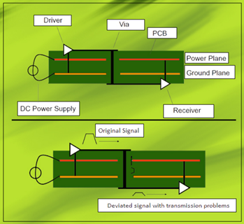
There will be varying levels of distortions with receiving information other than the initially sent information. The main reason behind it is the signals move from the source to the receiver. Impedance mismatch, reflections, ringing, crosstalk, jitter, and ground bounce are a few sources of this signal distortion. Such circumstances cause a circuit to become unstable, unreliable, and occasionally dysfunctional. The prime objective of a designer should be to reduce these elements as much as possible. So that the original signal may reach its destination with the least amount of distortion. Maintaining quality and limiting its unfavorable impacts on electrical circuits also require special attention.
Transmission line effects, impedance mismatch, high-speed switching characteristics, board material loss, and crosstalk are the most significant factors that influence the effectiveness of transmission in a PCB.
Transmission lines are conductive channels or links that may transport a signal between a transmitter and a receiver. Even the smallest passive printed circuit board (PCB) tracks are subject to transmission line effects during high-speed digital signal transmission. A transmission line's impedance is only resistive at low frequencies. Consequently, the following represents the transmission line's characteristic impedance at low frequencies.
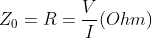
There, the Z represents the impedance of the line, which is the combination of ohmic resistance and reactance. Hence, this impedance measuring unit is ohms.
The inclusion of capacitive and inductive reactance causes the AC circuit characteristics to emerge at high frequencies in the transmission line. The complex component of the impedance is reactance. Accordingly, the following equations represent the transmission line impedances at higher frequencies:
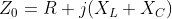
Here, the inductive reactance, denoted by the symbol and capacitive reactance, represented by. Are, directly and indirectly, proportional to frequency, respectively.
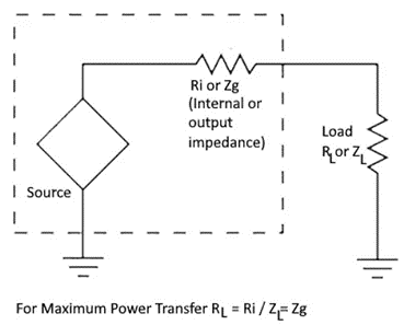
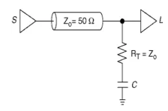
The impedance matching circumstance is equivalent to the transmission line effects. The load impedance of the output port must match the characteristic impedance or the internal impedance of the circuit to maximize signal coupling between the two ports. However, not all signal power will be subject to coupling when there is a mismatch between these impedances; instead, some signals will reflect into the transmission line. This results in a standing wave in the transmission line, which generates ringing, overshoot, undershoot, and stair-step waveforms. These factors significantly impact signal integrity.
The PCB selection of materials impacts the transmission of signals. Attenuation causes signal losses to happen. The dielectric material is a crucial component of PCB. The molecules in the dielectric medium are stimulated at high frequencies. Some of the signal energy is absorbed by exciting molecules, which results in signal loss. This scenario is known as dielectric absorption. By carefully choosing the PCB's dielectric material, this may be decreased.
The skin effect is an additional problem with signal transmission over conducting wires. The signal power often only travels on the conductor's surface at very high frequencies. The result is a reduction in the effective conductive area. Signal attenuation results from any surface imperfections on the conductor. Thus, Inductive reactance increases due to self-inductance caused by signals moving over the conductor's surface. widening the conducting surface will reduce the skin effect.
Mutual inductance and mutual capacitance cause crosstalk in a PCB. A magnetic field forms around a transmission wire, conveying a signal power. The signal energy is coupled when parallel lines are employed in a PCB close to one another due to magnetic coupling between the two lines. Mutual inductance occurs when a magnetic field in one line links to another line adjacent to it, and the inductance changes as the original line's current changes. The coupling of the electrical fields among the adjacent lines causes the mutual capacitance, which is proportional to the rate of change in voltage at the signal driver end. Plus, crosstalk lowers the quality as well.
High-speed simultaneous switching may influence the signal's integrity. The charges built up in the load capacitors are linked to the device when a large number of outputs on a PCB go from logic high to low. As a result, the load capacitors discharge, causing a sizeable transient current to flow into the device. Due to the coupling of this current to the ground, a low-voltage signal is established between the device board and the ground. This is referred to as a "ground bounce." The output terminals will get incorrect data due to this ground bounce (consistently high).
Here we have to be concerned about the factor or the sources that cause the generation of signal integrity. The remedies for this cause are as follows.
A PCB's signal integrity affects its dependability. The demand for low power consumption and small device sizes are two of the most crucial specifications in today's PCB designs. As this essay has highlighted, planning signal integrity during the early phases of planning will be far more effective than planning its later physical design.
Still, need help? Contact Us: support@nextpcb.com
Need a PCB or PCBA quote? Quote now


 Surface

