
 NextPCB Capabilities
Printed Circuit Boards
NextPCB Capabilities
Printed Circuit Boards
 PCB Assembly
 Layer Buildup
 SMD-Stencils
 PCB Design-Aid & Layout
 Mechanics
 Quality
 Drills & Throughplating
 Factory & Certificate
 PCB Assembly Factory Show
Certificate
PCB Assembly Factory Show
Certificate
Support Team
Feedback:
support@nextpcb.com


Vias have become essential features of double-sided printed circuit boards and as PCB fabrication capabilities have improved and demand for small powerful electronics has grown, the range of via sizes and types have grown as well. Here we attempt to cover every via type, when you would use them in your PCB design, what they look like in PCB manufacturing files or Gerber files and how they influence the cost of producing your PCBs.
Table of Contents
PCB vias are small copper-plated holes that serve the purpose of transferring electrical signals from one conductive layer to another. They are typically made by drilling holes in the PCB substrate early in the PCB production cycle. When the boards are sunk in the copper bath, the walls of the hole are plated over to form vias.
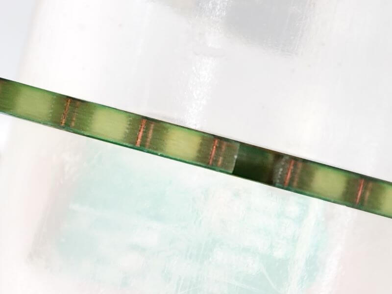
Cross section of a PCB board (sandwiched between acrylic blocks) showing the copper via barrels
Structurally, vias and through-holes are the same and are produced in the same way. The major difference is their purpose. Vias are used for conducting signals to other layers whereas plated through holes or PTHs, are required to solder through hole parts such as through-hole resistors, headers, connectors etc. to the boards and connect them to the onboard circuitry if necessary.
Since the plating process will decrease the diameter of the hole slightly, PCB CAM engineers will use a larger drill bit to compensate. This ensures that designers get the hole sizes they prescribed in the PCB Gerber and drill files. For vias, this is not necessary as the final diameter is not as important.
Typically, plated holes smaller than 0.5mm in size are considered vias although it can sometimes be hard to tell with smaller and smaller components coming onto the market.
Through-hole vias are standard vias that go through the entire board, connecting all layers with the via 'barrel'. In the exported Gerber files, vias consist of filled pads present on connected copper layers with a drill hole centered in the middle.
In inner layers where no electrical connection to the via is required, the PCB EDA software should add antipads to these layers, which are clearances from the via drill or annular ring to the plane.
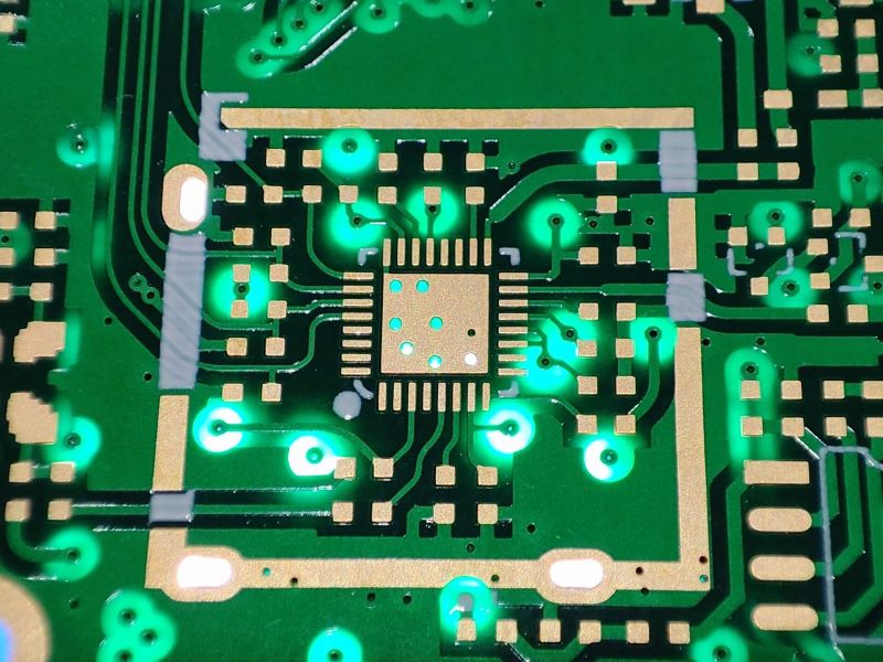
PCB lit up from behind showing large via antipads in the inner layers
Just about every PCB design nowadays will have plated holes of some sort (ignoring aluminum PCBs), so hole plating has become standard in the PCB production process. Don’t worry about additional costs for vias unless you add tiny vias or have hundreds on one board.
Pro Tip
Use 0.3mm size vias where possible as some fab houses may charge extra for 0.2mm drill holes since the smaller drill bit is more likely to snap and cause defects.
Blind and buried vias are named respectively due to the fact that blind vias are only visible on one side of the PCB board (one side is ‘blind’) and buried vias are not visible from the outside at all (they are ‘buried’ inside the boards). The vias are drilled at different production stages and are filled/plugged to ensure planarity.
In the context of these vias, the name ‘through-hole via’ given to regular vias becomes apparent, since they go completely ‘through’ the boards, unlike blind/buried vias.
Blind/buried vias are typically used where there is no board space for regular vias, for example, high-density designs. High-density designs incorporating blind/buried vias are often called High-Density Interconnects (HDI), and different levels of production difficulty are labeled HDI I, HDI II and HDI III, where HDI III is the most complicated and requires 3 additional lamination and plating cycles.
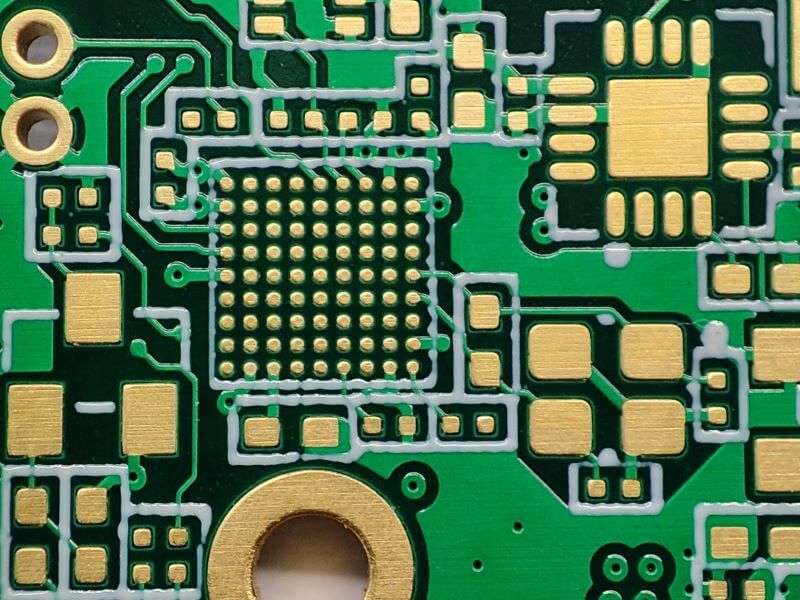
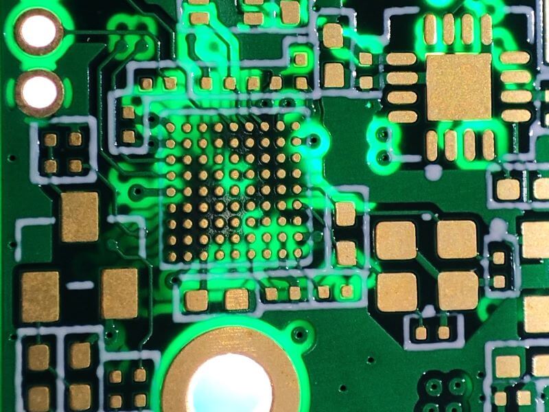
6-layer blind/buried via board showing the pads for a 0.4mm pitch BGA. The second photo shows the same area lit up from behind, showing traces on the inner layers running from the BGA's via-in-pads.
With blind/buried via design, new designers often fail to consider the manufacturing complexity associated with manufacturing blind/buried vias, and this can cause major setbacks if a board needs to be heavily redesigned.
Some combinations or blind/buried vias are not possible, and some may cause factor-fold increases in production costs. Blind/buried design is heavily tied in with custom board stack-ups, prepreg thicknesses, aspect ratios, microvias and via filling/plugging, so it is important for designers to do their research and consider other options if possible.
The simplest blind/buried via stack-up consists of blind vias connecting outer layers to adjacent inner layers and buried vias connecting these two inner layers, with no overlap between the blind/buried vias (no stacking). Production-wise, this consists of additional drilling, plugging and one additional lamination and plating cycle:
Since lamination is typically the longest step, the production time for HDI boards increases as well and can cause production costs to increase by several factors.
Most EDA software with blind/buried via capabilities will export all through, blind and buried vias into separate drill files and should label the files appropriately so the manufacturer knows which layers the vias connect.
For example, a six-layer board with the above blind/buried vias should export 4 drill files with the necessary labels:
(Following GTL-G2-G3-G4-G5-GBL layer naming)
Designers must communicate blind/buried via requests with their fabricator to obtain accurate quotations and ensure they are not mistakenly omitted.
Microvias are as the name suggests, are smaller than regular vias and have a 1: 1 diameter to depth board thickness to aspect ratio. They can be produced by laser drilling but this method can only penetrate very small thicknesses in the range of 0.1-0.25mm. As such, blind vias produced by the method described in the blind/buried via section are microvias and they both serve the purpose of getting the most out of the available board space. In more complex HDI designs, microvias can be staggered or stacked to provide additional interconnects.
Special laser drilling equipment and via filling machines are required to process microvias and such they are often regarded as advanced capabilities that many quickturn factories do not accommodate. Therefore, as with blind/buried vias, they should only be used if absolutely necessary.
By only using microvias (blind vias), it is possible to reduce manufacturing complexity slightly by eliminating the extra lamination step required for blind vias. Without blind vias, production only consists of one lamination and plating step as with regular multi-layer boards.
IPC-4761 (Design Guide for Protection of Printed Board Via Structures) defines 7 protection types or techniques for PCBs vias. Each type has different uses and can range considerably in cost. Choosing the right via protection type for an application should be part of a designer's strategy for reducing board defects, and increasing the reliability of the boards for the available budget.
Tenting vias is the most standard way of dealing with vias. During fabrication, no extra preparation is needed. Engineers simply follow the Gerber solder mask file to apply the solder mask and the vias will be covered over with solder mask. Whether or not the holes are fully covered depends on the size of the via, the type and the viscosity of the solder mask oil amongst other factors. Larger holes may not be fully covered or protected from debris entering the via, which may lead to corrosion and reliability issues.
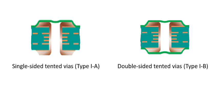
The downside to tented vias is that trapped air or liquids could expand and burst open the tent when exposed to high temperatures such as in a reflow oven. For this reason, some designers may choose to have open vias.
When solder mask openings are added to the vias, the via pads are exposed and treated with surface finish as with other exposed copper elements.
Designers may add solder mask openings to vias for testing purposes. However, opening vias leave them vulnerable to corrosion or accidental solder bridges. Designers should take care when opening vias, especially in high-density areas such as BGA pads where via openings could overlap, removing solder mask dams and increasing the risk of short circuits.
PCB board with OSP surface finish covered in opened vias
In some cases, designers simply do not know their vias are opened. PCB design software should have settings to dictate whether vias are opened or tented but the only way to make sure is to check the Gerber files. This is where a Gerber viewer such as HQ NextPCB’s free online Gerber viewer, HQDFM would help.
> See Practical DFM Checklist and HQDFM Practice
Not only can designers review the actual instructions they are sending to PCB manufacturers, with HQDFM, designers can analyze over 20 potential Design for Manufacturing (DFM) problems that could influence production or affect the performance of the boards. With one click, HQDFM will export a report detailing each issue and give suggestions on how to resolve them. Try it for free (no sign-up required).
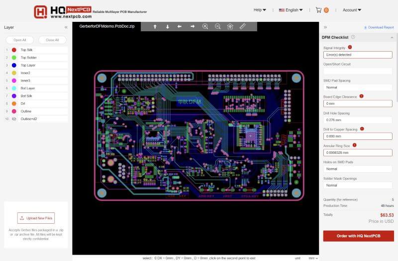
HQDFM Free Gerber Viewer from HQ NextPCB
Various filling and plugging options exist to protect vias. Filling materials typically include:
Solder mask
Non-conductive epoxy/resin
Conductive epoxy/resin
As defined by IPC, plugging and filling have specific definitions and should not be used interchangeably:
Plugging: Partial blocking of the via barrel
Filling: Complete filling of the via barrel with no gaps
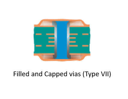
Capping: To plate the top vias with a solderable pad
With solder mask plugging, technicians push solder mask into the vias with an aluminum squeegee, then typically cover with solder mask as with tented vias. With this method, the vias are guaranteed to be plugged with solder mask, however, this does not remove gaps and air pockets.
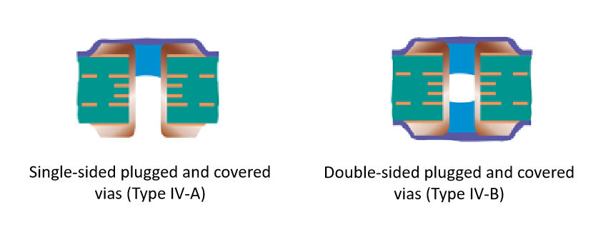
From the outside, all vias will be filled and appear dark (not transparent which is possible with tented vias).
For via filling, the vias are filled with either non-conductive or conductive resin, then the surface is ground flat and cleaned. This is followed by a separate electroplating step to produce planar pads on top of the vias. From the outside, filled and capped vias have the appearance of regular surface mount pads. The choice of filling depends on the purpose of the via.
Non-conductive resin fill is much more common and is used where vias are present on surface mount pads. If the vias are not blocked, solder will wick away into the cavity and away from the solder joint increasing soldering defects and the overall reliability of the board.
Such vias are often referred to as via-in-pads and are often necessary for high-density designs and escaping BGA (ball-grid-array) footprints that are too small to accommodate dog bones or fan-out routing. Due to manufacturing constraints, routing out 0.5mm and less pitch BGA pads is difficult-if not impossible without via-in-pads. Via-in-pads can also be useful in situations where trace length must be kept to a minimum for example to reduce the parasitic inductance and capacitance effect.
Vias filled with conductive epoxy are used to increase the thermal conductivity of the via. It is sparsely used as the cost of processing the vias is high and the increase in heat transfer is somewhat moderate. Other methods of dissipating heat that are much cheaper and more effective are usually considered.
Don’t get confused; filling with non-conductive resin does not mean the via is non-conductive or will pass a weaker signal. The via barrel is still present and the electrical signal passed is the same as regular vias.
> Recommend reading: When to Use Vias in PCB Design: An Engineer's Decision Guide
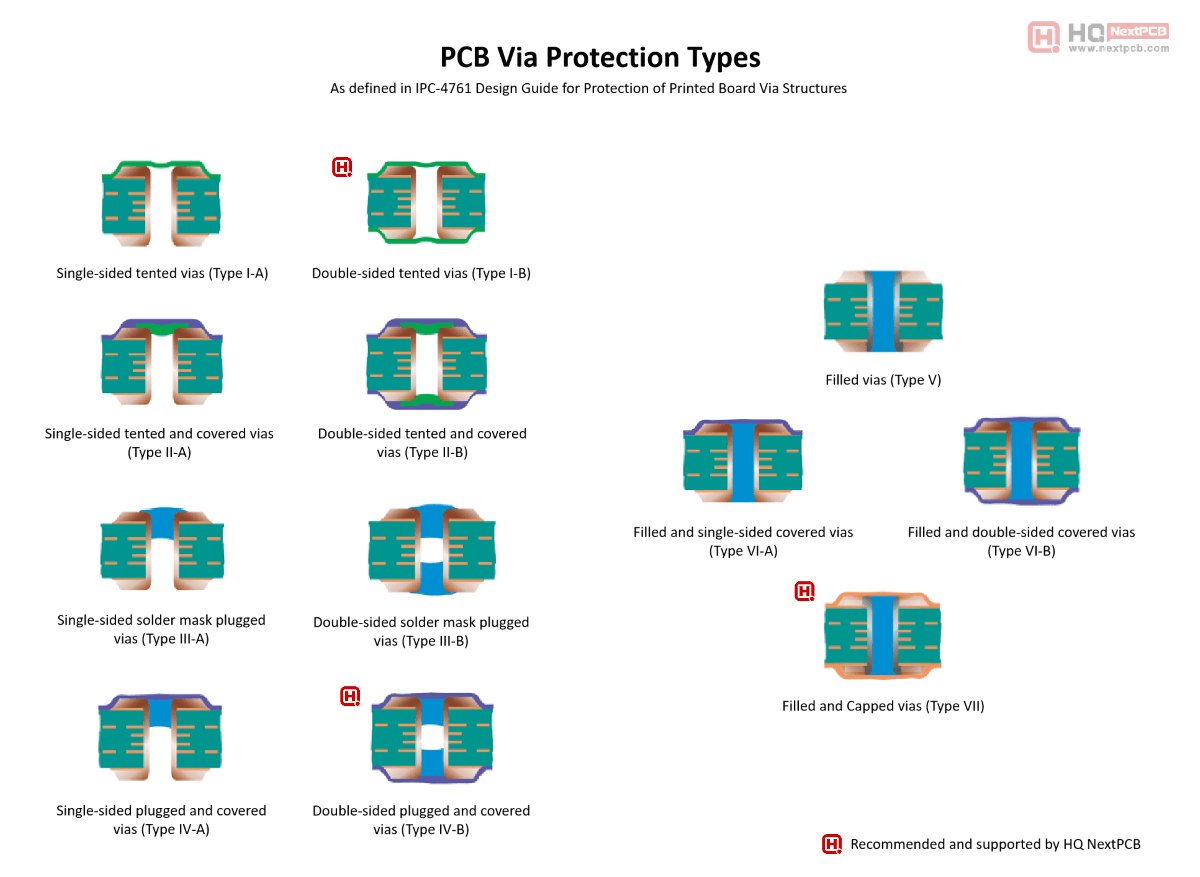
IPC specifies 7 different via protection types. The types with the H mark are supported by HQ NextPCB (click to enlarge)
HQ NextPCB can produce through, blind and buried vias, up to HDI III level designs, microvias and open, tented, solder mask plugged and tented vias (IV) and via filling with non-conductive resin (VII). All these via types and protection techniques are highly recommended by NextPCB and by using NextPCB’s smart instant quotation platform, you can add these to your board with a single click and see the price and lead time upfront.
As a PCB manufacturer specializing in high-reliability multilayer boards, you can count on your boards' vias withstanding the test of time when you choose HQ NextPCB.

Still, need help? Contact Us: support@nextpcb.com
Need a PCB or PCBA quote? Quote now


 Surface

