
 NextPCB Capabilities
Printed Circuit Boards
NextPCB Capabilities
Printed Circuit Boards
 PCB Assembly
 Layer Buildup
 SMD-Stencils
 PCB Design-Aid & Layout
 Mechanics
 Quality
 Drills & Throughplating
 Factory & Certificate
 PCB Assembly Factory Show
Certificate
PCB Assembly Factory Show
Certificate
Support Team
Feedback:
support@nextpcb.com


As digital data rates continue to accelerate into the multi-gigabit range, conventional manufacturing processes for plated through-hole (PTH) vias introduce signal integrity compromises. Controlled-Depth Drilling (CDD), universally known as back drilling, is a critical, specialized fabrication step necessary for modern high-layer count printed circuit board (PCB) designs.
Back drilling is the precise, mechanical removal of the unused conductive portion, or stub, of a PTH via barrel. This technique is strictly implemented to improve signal integrity (SI) by reducing reflection and interference caused by the unused via material. This overview details the technical necessity, manufacturing requirements, and critical trade-offs of implementing back drilling in advanced PCB designs.
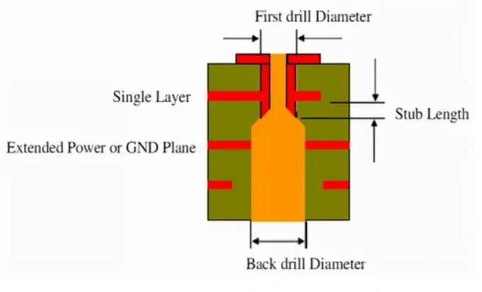
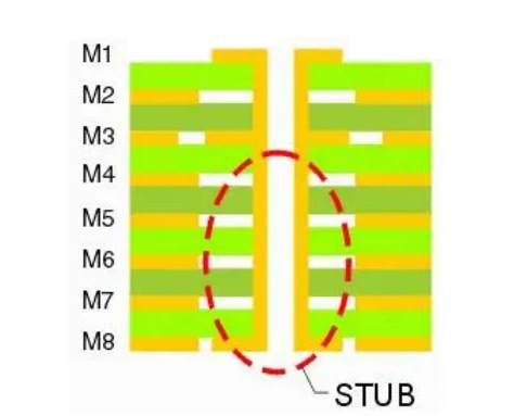
A via stub is the section of the copper plating in a PTH that extends beyond the required electrical path. For example, if a signal is routed from Layer 1 to Layer 4 in a 16-layer stack-up, the copper barrel spanning Layers 4 through 16 serves no function for that specific signal and constitutes the stub.
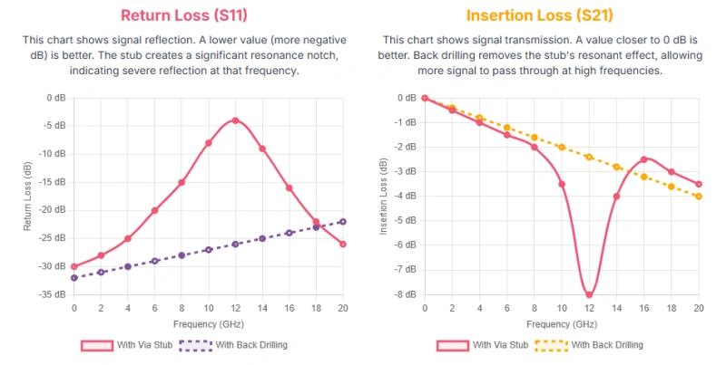
The entire PTH structure functions as a transmission line. When a high-speed signal leaves the via at the connection layer, the remaining, unutilized portion of the barrel becomes an unterminated transmission line. This unterminated end causes high-frequency energy to reflect back toward the signal source, severely compromising signal clarity at gigabit speeds.
At high frequencies, the electrical length of the via stub can easily approach a significant fraction of the signal's wavelength. In this condition, the stub acts as an unterminated antenna structure or a resonant circuit.
This resonant behavior causes three primary degradation mechanisms:
The resonant frequency is inversely proportional to the stub length (ls) and the dielectric constant (ϵr) of the PCB material, based on the quarter-wavelength (λ/4) resonance criterion:
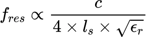
For modern, high-speed standards, the impact is severe. For instance, in a common 0.063'' thick FR-4 board, if a signal only spans a few layers, the remaining stub length can easily exceed 33 mils. For NRZ signaling at 28 Gbps, engineering guidance, often derived from simulation, suggests controlling the maximum stub length to ≤12 mils (0.012 inches). Back drilling is therefore a method often employed to push the resonant frequency out of the active signal bandwidth.
Determining whether back drilling is necessary for a design relies on the signal frequency and the physical length of the potential stub relative to the signal wavelength. Back drilling is commonly employed and often necessary when signal degradation due to stubs is substantial, which occurs in channels operating at multi-gigabit speeds (multi-Gbps and above), on thicker boards, or when the unmitigated via stub length exceeds critical thresholds (e.g., >15 mils for PCIe Gen 4). As the signal frequency increases, the electrical length of the stub approaches a larger fraction of the signal wavelength, making the reflection effect more significant. Back drilling is particularly vital in high-density backplanes and midplanes where alternative stub-reduction techniques may be geometrically unviable or cost-prohibitive.
To meet the stringent link budget and signal integrity (SI) compliance requirements of modern communication standards—such as tight jitter and insertion loss targets—back drilling or an equivalent stub-reduction technique is frequently required in high-layer count or backplane designs.
For example, high-speed digital interfaces such as PCIe Gen 5 (32 GT/s) and PCIe Gen 6 (64 GT/s PAM4), and high-throughput networking standards like 10 Gb/s Ethernet and 100G/400G Ethernet require stub mitigation to meet their ultra-short residual stub length specifications (often <3 mils). While standards rarely mandate a specific manufacturing process, engineering guidance, such as that for PCIe Gen 4.0, recommends back drilling when the via stub length exceeds 15 mils, confirming that CDD is a key solution when the stub becomes a critical link bottleneck. The decision to use back drilling is thus determined by the channel's signal integrity requirements and thickness constraints.
The necessity of back drilling is exacerbated by board thickness. Back drilling is most effective and crucial on thicker boards, typically those ≥2 mm (0.079 inches), where the inherent length of the via stub is longer and thus more likely to cause significant SI problems.
To achieve compliance with high-speed standards, the target residual stub length must be aggressively minimized.
The industry standard nominal target stub length (H1) is often specified as 0.007" ± 0.005" (7 mils ± 5 mils). The achievable range for residual stub length (from the Minimum Necessary Connection (MNC) layer to the drill stop) in high-end manufacturing is often cited as 0.002" to 0.012". Achieving the required performance for cutting-edge standards often necessitates achieving the absolute physical minimum stub length (H2), generally 0.002" (2 mils). Meeting this constraint requires depth tolerances as tight as ±0.002" during the fabrication process.
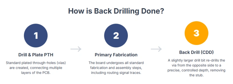
Back drilling is performed as a specialized post-plating fabrication step. After the PTHs have been drilled and plated with copper, a secondary drilling operation is executed.
Successful CDD implementation requires strict adherence to Design for Manufacturability (DFM) rules to ensure both performance and reliability.
|
DFM Parameter |
Guideline (Imperial) |
Purpose |
|
Nominal Target Stub (H1) |
0.007"±0.005" |
Standard residual length goal |
|
Absolute Minimum Stub (H2) |
0.002" |
Minimum functional stub length |
|
Back Drill Clearance (C1) |
≥0.006" min; ≥0.010" preferred |
Minimum distance to adjacent copper features |
|
Back Drill Size Over Primary |
Primary Drill + 0.008" to 0.010" |
Ensures complete removal of conductive plating |
|
Depth Tolerance |
±0.002" (typical) to ±0.005" |
Required Z-axis precision |
The use of an oversized drill bit necessitates careful planning for the Back Drill Clearance (C1) to prevent the drill from damaging adjacent traces or copper features. While a minimum clearance of 0.006” is cited, industry best practice often recommends a planar/trace clearance of ≥0.010" (10 mils) to mitigate risk, especially in high-density areas. This requirement imposes a local penalty on routing density near the via.
When addressing high-speed SI or routing density, engineers typically compare Back Drilling with Blind Vias and Buried Vias.
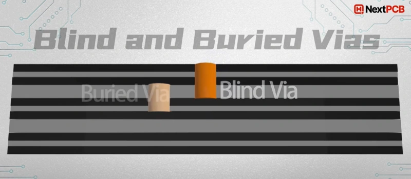
> Recommend reading: Blind Vias and Buried Vias: What Is the Difference in PCB?
|
Feature |
Back Drilling (CDD) |
Blind Vias |
Buried Vias |
|
Primary Goal |
Signal Integrity (Stub Removal) |
Space Efficiency (Outer Layer) |
Space Efficiency (Inner Layers) |
|
Signal Performance |
Highly effective in reducing reflections and loss; provides competitive SI performance compared to other stub-reduction techniques. |
Short signal path reduces distortion. |
Shorter paths minimize signal loss; enable maximum routing density. |
|
Space Utilization |
Does not free up surface space. |
Frees up routing space on the opposite surface. |
Frees up maximum space on both outer surfaces. |
> Recommend reading: What is a Via in PCB Design and Every Via Type
The manufacturing cost premium associated with back drilling makes it the most economical solution for achieving high-speed signal integrity performance by addressing the stub issue directly.
|
Via Type |
Manufacturing Complexity |
Cost Premium |
|
Back Drilling (CDD) |
Added drilling pass; high Z-axis precision. |
Moderate: Adds an additional, precise drilling step. |
|
Blind Vias |
Requires advanced laser drilling and complex plating cycles. |
High: Significantly more expensive than back drilling. |
|
Buried Vias |
Highest complexity; requires sequential lamination cycles (multiple press and drill steps). |
Highest: Can be substantially more expensive than standard vias due to sequential lamination. |
For high-layer count systems like backplanes, where the cost of sequential lamination for hundreds of vias is prohibitive, back drilling offers the most practical and cost-effective approach for maintaining signal bandwidth at 10 Gbps or more.
The process requires extreme Z-axis precision. The primary risks stem from dimensional error:
Given the internal nature of stub removal, specialized testing is mandatory:
Q: What is the main purpose of back drilling?
A: The primary goal is to remove the unused copper barrel (via stub) of a plated through-hole (PTH). This prevents the stub from acting as a resonant circuit or an unterminated antenna, thereby improving signal integrity, reducing reflections, and enhancing channel performance in high-speed applications.
Q: When does a design require back drilling?
A: Back drilling is commonly required in channels operating at multi-gigabit speeds, particularly on thicker boards, or when via stub length exceeds critical thresholds (e.g., >15 mils for PCIe Gen 4). It is an essential engineering practice for meeting the performance requirements of standards like PCIe Gen 5/6 and 100G/400G Ethernet.
Q: What is the target residual stub length?
A: The industry nominal target for the residual stub length (H1) is 0.007”±0.005” (7 mils ± 5 mils). However, to meet the performance requirements of the fastest standards, the target stub length must often be reduced to less than 3 mils (0.003 inches).
Q: How does the cost of back drilling compare to blind or buried vias?
A: Back drilling is typically the most cost-effective high-speed SI solution. It adds an extra precise drilling step (moderate cost increase), but it is significantly less expensive than blind vias or buried vias, which require complex laser drilling or multiple sequential lamination cycles.
Q: What are the primary manufacturing risks associated with CDD?
A: The main risks are over-drilling (drilling too deep, potentially severing the functional connection) and under-drilling (leaving an unacceptable residual stub that degrades signal performance). Precision systems aim for depth tolerances as tight as ±0.002” to mitigate these risks.
Back drilling, or Controlled-Depth Drilling (CDD), is a precise, indispensable manufacturing technique central to modern high-speed PCB fabrication. Its role is to mitigate the devastating effects of via stubs, which behave as unterminated transmission lines that compromise signal integrity, particularly in multi-gigabit/high-frequency interconnects. To meet the stringent signal integrity and link budget requirements of high-speed systems like PCIe Gen 5/6 and 100G/400G Ethernet, engineers find it common and often necessary to employ stub mitigation methods. Back drilling is the primary method used to remove the unused copper barrel to leave a residual stub length often below 10 mils—and critically, below 3 mils—thereby ensuring cleaner, more reliable data transmission and achieving high-performance compliance.
The choice to implement CDD is fundamentally a strategic trade-off. For complex, high-layer count architectures such as backplanes, telecommunication switching equipment, and data center servers, back drilling offers the most pragmatic balance of signal performance and cost. It provides superior signal integrity correction compared to standard PTHs at only a moderate manufacturing cost penalty (adding an additional drilling step), making it significantly more economical than the complex, high-cost manufacturing required for blind or buried vias (which necessitate laser drilling or multiple sequential lamination cycles).
As data rates continue to accelerate, demanding increasingly stringent tolerances and pushing the required residual stub length ever closer to the 2 mil manufacturing minimum, the precision and rigor required in the back drilling process will only grow. CDD remains a cornerstone technology, essential for meeting the performance demands of cutting-edge applications where signal degradation is not merely a performance issue but a critical determinant of system reliability.
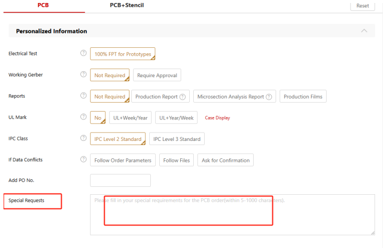
Note: If your PCB design requires back drilling, be sure to specify this clearly in the Special Requests section of the pricing page.
> Recommend reading: PCB Assembly - The Most Comprehensive Guide | NextPCB

Still, need help? Contact Us: support@nextpcb.com
Need a PCB or PCBA quote? Quote now


 Surface

